UG-570 AD9361 Reference Manual
| Page 106 of 128
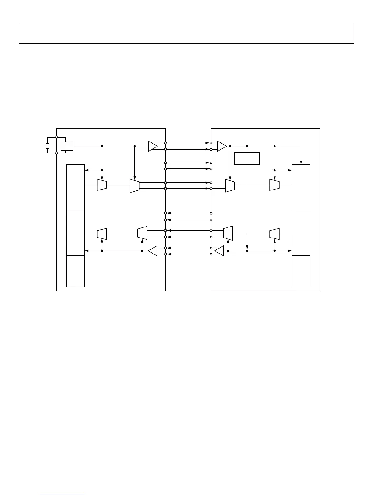
LVDS MODE DATA PATH AND CLOCK SIGNALS
The following information describes operation of the AD9361
data path in low voltage differential signal (LVDS) mode
(ANSI-644 compatible). The AD9361 data path interface uses
parallel data buses (P0 and P1) to transfer data samples between
the AD9361 and the BBP. The bus transfers are controlled using
simple hardware handshake signaling. In LVDS mode, both
buses are used with differential LVDS signaling.
The AD9361 LVDS interface facilitates connecting to custom
ASICs and FPGAs that have LVDS capability. LVDS interfaces
are typically used when a system needs superior switching
performance in noisy environments and higher data rates than
a standard CMOS interface can provide. When utilizing LVDS
mode, it is recommended to keep all trace lengths no longer
than 12 inches and to keep differential traces close together and
at equal lengths.
Fig
ure 78. AD9361 Data Path, LVDS Mode
DATA_CLK_P
RX_FRAME_P
TX_P[5:0]
FB_CLK_P
RX
DATA
RX
DATA
TX
DATA
TX
DATA
CTRL CTRL
PLL
FEEDBACK
CLK GEN
AD9361
BBP
TX_FRAME_P
RX_P[5:0]
DATA_CLK_N
RX_FRAME_N
RX_N[5:0]
TX_FRAME_N
TX_N[5:0]
FB_CLK_N
11668-079

 Loading...


