UG-570 AD9361 Reference Manual
| Page 82 of 128
AuxADC/AuxDAC/GPO/TEMP SENSOR
OVERVIEW
This section describes operation of the auxiliary features
available in the AD9361. These features help simplify system
tasks and lower overall system cost. They include two 10-bit
auxiliary DACs, one 12-bit auxiliary ADC, an internal tempera-
ture sensor, and four general-purpose output (GPO) pins.
AuxDAC
The two AuxDACs are 10-bit general purpose DACs. Each is
capable of sourcing 10 mA. For stability, place a 0.1 µF capacitor
on the output of each AuxDAC. SPI writes enable the AuxDAC.
The AuxDAC may be set for manual operation or be set to
automatically toggle during TDD operation to reduce control
required from the B B P. The AuxDAC is configured using the
ad9361_auxdac_setup function. By default, the AuxDACs are
disabled when the device is first powered up.
In certain applications, it is desirable to delay the AuxDAC
transition after the enable signal transitions. Each AuxDAC has
its own receive and transmit mode delay setting in Register
0x30 through Register 0x33. Each LSB equals approximately
1 µs. Register 0x3A must be set based on your reference clock
to program a 1 µs delay. Set Bits[D6:D0] to the number of
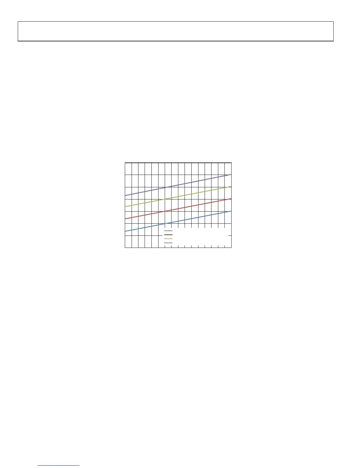
reference clock cycles per µs minus one. Figure 55 shows the
AuxDAC code vs. output voltage for four different reference
voltage settings for AuxDAC 1.
Figure 55. AuxDAC Output Voltage vs. Register 0x18 through Register 0x1B Code
3.5
0
0.5
1.0
1.5
2.0
2.5
3.0
0 128 256 384 512 640 768 896 1024
OUTPUT VOLTAGE (V)
AUXDAC CODE (Decimal)
REFERENCE VOLTAGE = 2.0V
REFERENCE VOLTAGE = 1.5V
REFERENCE VOLTAGE = 1.0V
REFERENCE VOLTAGE = 2.5V
11668-056

 Loading...


