UG-570 AD9361 Reference Manual
| Page 126 of 128
Rx LO FREQUENCY DEVIATIONS DUE TO POWER
SUPPLY TRANSIENTS
The AD9361 is a transceiver that can operate in TDD or in
FDD mode. In FDD mode, there is a need to dynamically
change the transmit power when the receivers are on and
receiving data. This means that the load that the part presents to
the power supply changes, giving rise to transients on the power
supply line. The amplitude and the response time of these
transients depend on board layout and the regulator used to
supply power. These power supply transients are detrimental to
the receiver performance until the transient has died down.
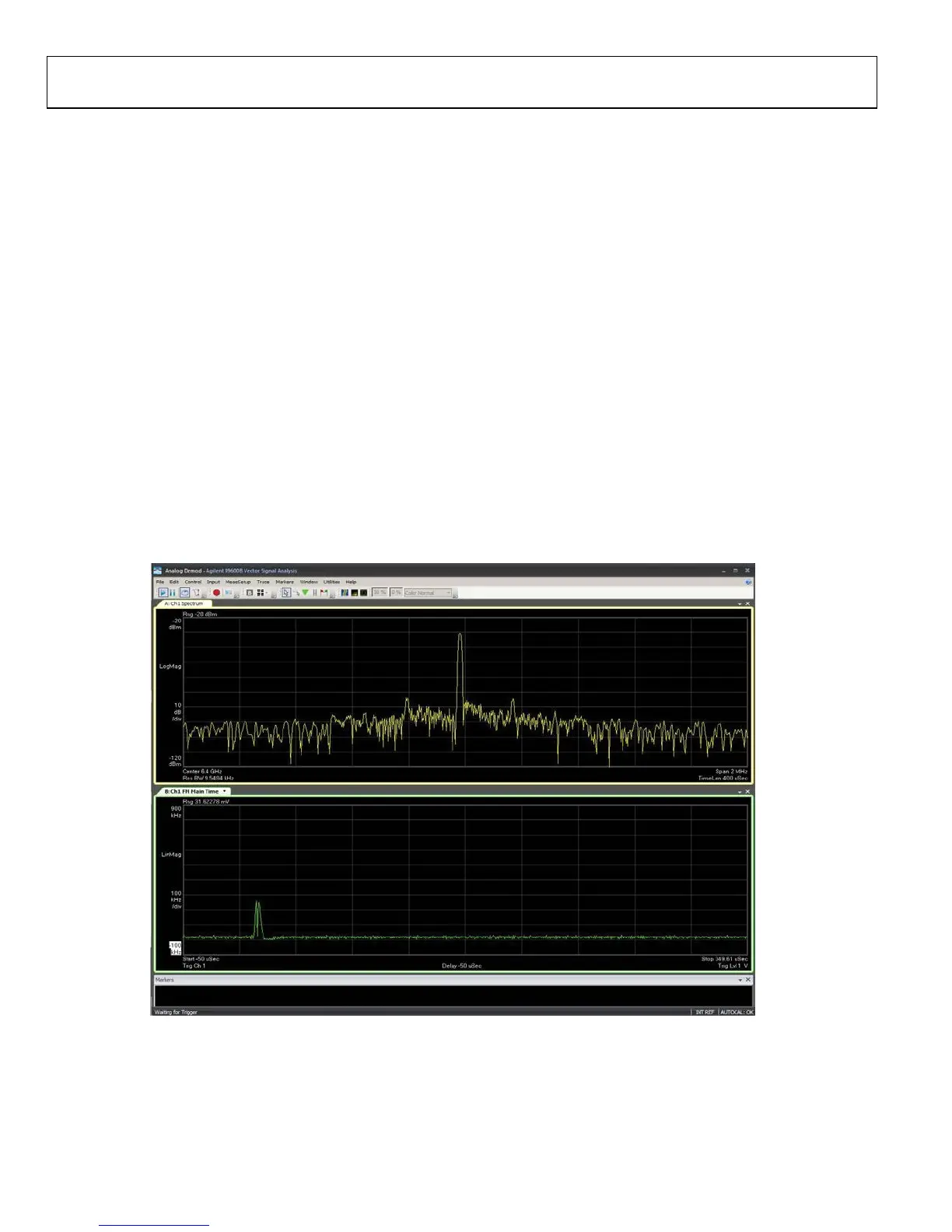
Figure 92 shows the instantaneous deviation in the Rx VCO
frequency due to a voltage transient on the 1.3 V supply. During
this experiment, The AD9361 was in FDD state. The Channel 1
spectrum in Figure 92 is the Rx VCO leakage from the Rx pin
when the Rx LO is 800 MHz. Channel 2 is a FM demodulation
of Channel 1. This means that Channel 2 will show the
instantaneous changes in VCO frequency. The spectrum
analyzer is triggered on the TXNRX signal that turns the
transmitter ON or OFF. This environment simulates the worst
case VCO frequency deviation that can occur on the Rx synth.
The blue trace in Figure 93 shows the voltage transient on the
1.3 V line when the transmitters turn ON. The magenta trace is
the Vtune voltage of the Tx VCO that is probed on the Tx EXT
LO line and the green trace is the Vtune voltage of the Rx VCO
that is probed on the Rx EXT LO line. The instantaneous
frequency deviation shown in Figure 92 is a direct cause of the
instantaneous change in the Vtune voltage. Screenshots in
Figure 92 and Figure 93 were taken simultaneously on one
trigger. The experiment described previously was done with the
ADP1706-1.3V LDO powering the 1.3 V supply.
This issue can be mitigated by powering the Rx synth, Tx synth,
Rx LO and Tx LO supplies from a different LDO. This approach
helps in isolating the synthesizers from the transients on the
1.3 V supply. Figure 94 shows the frequency kick when the Rx
synth, Tx synth, Tx LO, and Rx LO supplies are powered up
externally. The frequency kick decreases to one third of its
initial amplitude. Figure 95 shows the voltage kick on the 1.3 V
supply and the consequent response of Vtune voltage of the Tx
VCO (magenta) and the Vtune voltage of the Rx VCO (green).
Fig
ure 92. Instantaneous Rx VCO Frequency Deviation Seen Due to a Voltage Transient on the 1.3 V Supply

 Loading...


