AD9361 Reference Manual UG-570
| Page 83 of 128
AuxADC
The AuxADC is a 12-bit auxiliary converter with an input level
range 0 V to 1.3 V with an adjustable conversion time. The
AuxADC is configured using the ad9361_auxadc_setup
function. The AuxADC allows monitoring of desired voltages
such as a PA power detector or an external temperature sensor.
A small value capacitor (680 pF) may be placed on the
AUXADC pin to improve noise performance. The AD9361 also
includes an internal temperature sensor that can be measured
using the AuxADC. Note that the AuxADC can only be used to
measure either the internal temperature or the voltage on the
AUXADC pin at a time.
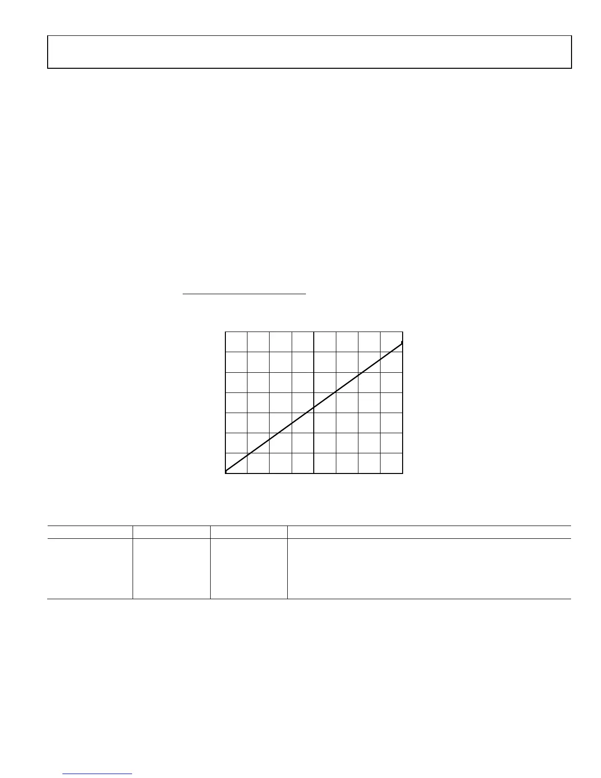
Figure 56 shows the AuxADC code vs. input voltage. The
AuxADC is off by default. The AuxADC clock is generated by
dividing the baseband PLL frequency. Equation 21 and
Equation 22 determine the AuxADC clock frequency and the
decimation rates.
The AuxADC output is read from Register 0x1E (D7:D0) and
Register 0x1F (D3:D0). To capture the voltage on the
AUXADC pin, the decimation filter clock should be routed on
the CTRL_OUT0 pin. To select the AuxADC decimation clock
on the CTRL_OUT0 pin write Register 0x35 to Register 0x1E.
Data from Register 0x1E (D7:D0) and Register 0x1F (D3:D0)
can be latched on the falling edge or on the rising edge of
decimation clock coming out of the CTRL_OUT0 pin. The SPI
reads must occur before the edge on the control out signal
toggles again.
The register settings used during the ramp test shown in
Figure 56 are shown in Table 45.
]0:5[1 DividerClockAuxADC
FrequencyBBPLL
FrequencyClockAuxADC
(21)
AuxADC Decimation = 256 × 2
AuxADC Decimation[2:0]
(22)
Figure 56. AuxADC
Code vs. Input Voltage
Table 45. Example Code for AuxADC Set Up
Command Address(hex) Data(hex) Comment
SPI Write 0F 4 Disable temp sensor read back
SPI Write 1C 63 Set the AuxADC clock frequency to BBPLL/36
SPI Write 1D 0 Enable AuxADC and set decimation to 256
SPI Write 35 1E Select AuxADC valid on control out [0]
SPI Write 36 FF Enable all control out pins
1.4
0
0.2
0.4
0.6
0.8
1.0
1.2
0 512 1024 1536 2048 2560 3072 3584 4096
VOLTAGE (V)
AUXDAC CODE (Decimal)
11668-057

 Loading...


