AD9361 Reference Manual UG-570
| Page 73 of 128
CONTROL OUTPUT
OVERVIEW
The AD9361 provides real-time status information on up to
eight dedicated pins. Information such as when calibrations are
running and the state of the overload detectors in the receive
signal path are just a few of the many options available. This
section describes the signals and their behavior in detail while
also showing how to program the registers so that the desired
signals are available on the appropriate balls. This section also
provides some information about how a BBP could use the
signals in an application. The control outputs are configured
using the ad9361_ctrl_outs_setup function.
As shown in Table 44, the control output signals are mapped as
a table. The Control Output Pointer selects the row (address)
that will be sent to the output pins. And the bits in Control
Output Enable individually select which output pins will be
active. The AD9361 will hold low any pins not enabled.
Some internal signals are available on more than one
combination of Control Output Pointer and Control Output
Enable. For example, to enable a control output that indicates
that the Rx1 gain has changed, the Control Output Pointer
register could be set to 0x08 and the Control Output Enable
register would then be set to 0x10. The same signal is also
available by setting Control Output Pointer to 0x05 and Control
Output Enable to 0x40 or alternatively with Control Output
Pointer set to 0x1E and Control Output Enable set to 0x04. Any
one of these options is valid. The BBP can only monitor the
signals in one row at a time because Register Control Output
Pointer can only have a single value loaded at any given time.
Thus, selecting one over the other depends on which other
signals the BBP needs to monitor simultaneously. From the
example, if the BBP also needs to know when the AuxADC
word is valid, only the option of setting Control Output Pointer
to 0x1E will allow this combination of the two signals. In this
case, Control Output Enable would need to be set to 0x05. The
BBP can also set more of the bits in Control Output Enable even
if it does not monitor those signals.
Some of the signals are helpful in a production system while
some others are useful for debug. In either case, Analog Devices
recommends connecting the AD9361 control outputs to BBP
inputs on the BBP so that the BBP can monitor real-time
conditions in the AD9361.
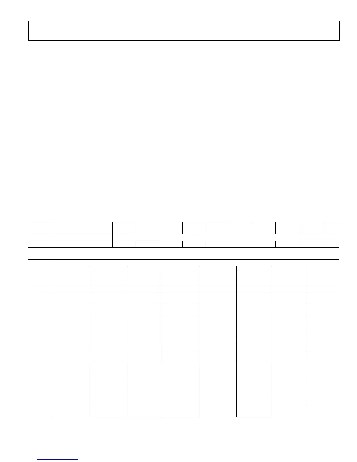
Table 43. Control Output Bit Descriptions
Register
Address Name D7 D6 D5 D4 D3 D2 D1 D0 Default R/W
0x035 Control Output Pointer Control Output Pointer[7:0] 0x00 R/W
0x036 Control Output Enable En ctrl7 En ctrl6 En ctrl5 En ctrl4 En ctrl3 En ctrl2 En ctrl1 En ctrl0 FF R/W
Table 44. Control Output Table
Register
0x035
Control Output Bit Position
D7 D6 D5 D4 D3 D2 D1 D0
00 Cal Done Tx CP Cal Done Rx CP Cal
Done
Rx BB Filter
Tuning Done
Tx BB Filter
Tuning Done
Gain Step Cal
Busy
Rx Synth VCO
Cal Busy
Tx Synth VCO
Cal Busy
01 Tx RF PLL Lock Rx RF PLL Lock BBPLL Lock 0 0 0 0 0
02 BB DC Cal Busy RF DC Cal Busy CH1 Rx Quad
Cal Busy
CH1 Tx Quad
Cal Busy
CH2 Rx Quad
Cal Busy
CH2 Tx Quad
Cal Busy
Gain Step Cal
Busy
Tx Mon Cal
Busy
03 CH1 ADC Low
Power
CH1 Lg LMT
Ovrg
CH1 Lg ADC
Ovrg
CH1 Sm ADC
Ovrg
CH2 Low Power CH2 Lg LMT
Ovrg
CH2 Lg ADC
Ovrg
CH2 Sm ADC
Ovrg
04 CH 2 Rx Gain[6] CH2 Rx Gain[5] CH2 Rx
Gain[4]
CH2 Rx Gain[3] CH2 Rx Gain[2] CH2 Lg LMT
Ovrg
CH2 Lg ADC
Ovrg
CH2 Gain
Lock
05 CH2 Gain
Change
CH1 Gain
Change
CH2 Low
Power
CH2 Lg LMT
Ovrg
CH2 Lg ADC
Ovrg
CH2 Gain Lock CH2 Energy
Lost
CH2 Stronger
Signal
06 CH1 Low Power CH1 Lg LMT
Ovrg
CH1 Lg ADC
Ovrg
CH1 Rx Gain[6] CH1 Rx Gain[5] CH1 Rx
Gain[4]
CH1 Rx
Gain[3]
CH1 Rx
Gain[2]
07 CH1 Low Power CH1 Lg LMT
Ovrg
CH1 Lg ADC
Ovrg
CH1 Sm ADC
Ovrg
CH1 AGC SM[2] CH1 AGC
SM[1]
CH1 AGC
SM[0]
CH1 Gain
Lock
08 CH1 Stronger
Signal
CH1 Gain Lock CH1 Energy
Lost
CH1 Gain
Change
CH2 Stronger
Signal
CH2 Gain Lock CH2 Energy
Lost
CH2 Gain
Change
09 RxOn CH1 RSSI
Preamble
Ready
CH1 RSSI
Symbol Ready
TxOn CH2 RSSI
Preamble
Ready
CH2 RSSI
Symbol Ready
0A CH1 Tx Int3
Overflow
CH1 Tx HB3
Overflow
CH1 Tx HB2
Overflow
CH1 Tx QEC
Overflow
CH1 Tx HB1
Overflow
CH1 Tx FIR
Overflow
CH1 Rx FIR
Overflow
0B Cal Seq State[3] Cal Seq State
[2]
Cal Seq State
[1]
Cal Seq State
[0]
ENSM[3] ENSM[2] ENSM[1] ENSM[0]

 Loading...


