UG-570 AD9361 Reference Manual
| Page 62 of 128
Rx SIGNAL PATH INTERFACE
The AD9361 LNA devices (1A, 1B, 1C, 2A, 2B, 2C) are
functional for the full 70 MHz to 6.0 GHz receive frequency
range. When operating at or below 3 GHz, any LNA input port
will provide optimal performance. When operating above
3 GHz, utilize the Rx1A and Rx2A LNA input ports for optimal
performance. All three LNAs provide differential inputs that
can also be configured as single-ended inputs (either side of the
differential input can be used as a single ended input). It is
recommended to configure the LNA inputs in differential mode
to achieve best noise figure and even order distortion (IP2)
performance. The LNA input pins have DC bias (~ 0.6 V
dc
)
present on them and may need to be ac-coupled depending on
the common-mode voltage level of the external circuit. The
maximum safe input level is +2.5 dBm peak (single-ended, ideal
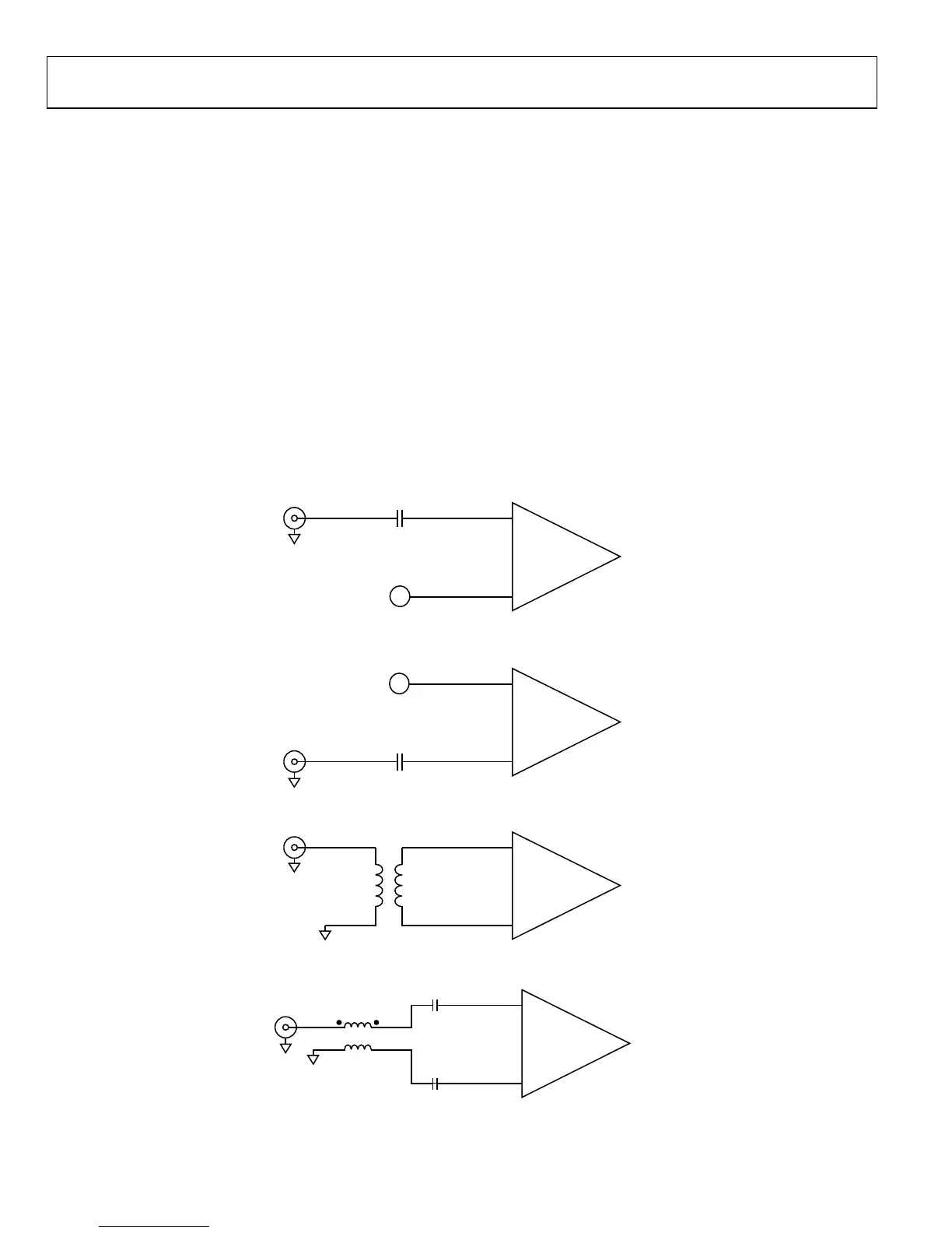
match, 50 Ω source). Figure 34 shows basic single ended and
differential interface configurations. Note that matching
networks will most likely be required to achieve optimum
performance.
Given a single-ended operation mode, a positive side
connection is delineated by the _P at the end of the Rx input
port name and a negative side connection is delineated by the
_N at the end of the Rx input port name.
The Rx differential input impedance varies over frequency and
is shown in Figure 38 through Figure 47. The reference plane
for this data is the AD9361 ball pads.
Note that Zo within the graph marker sections is 50 Ω.
Figure 34. AD9361 Rx Input Interface Circuit—Single-Ended Interface to the Negative Side of the Differential Input
Figure 35. AD9361 Rx Input Interface Circuits—Single-Ended Interface to the Positive Side of the Differential Input
Figure 36. AD9361 Rx Input Interface Circuits—Differential Interface Using a Transformer
Figure 37. AD9361 Rx Input Interface Circuits—Differential Interface Using a Transmission Line Balun
C
C
RxA_N
RxA_P
LNA
OPEN,
SHORT,
OTHER BAND/PATH
11668-035
C
C
RxA_P
LNA
RxA_N
OPEN,
SHORT,
OTHER BAND/PATH
11668-036
RxA_N
RxA_P
LNA
C
C
C
C
11668-038

 Loading...


