AD9361 Reference Manual UG-570
| Page 105 of 128
DATA BUS IDLE AND TURNAROUND PERIODS
(CMOS)
The P0_D[11:0] and P1_D[11:0] bus signals are usually actively
driven by the BBP or by the AD9361. During any idle periods,
the data bus values are ignored by both components. Both
ports, however, must have valid logic levels even if they are
unused.
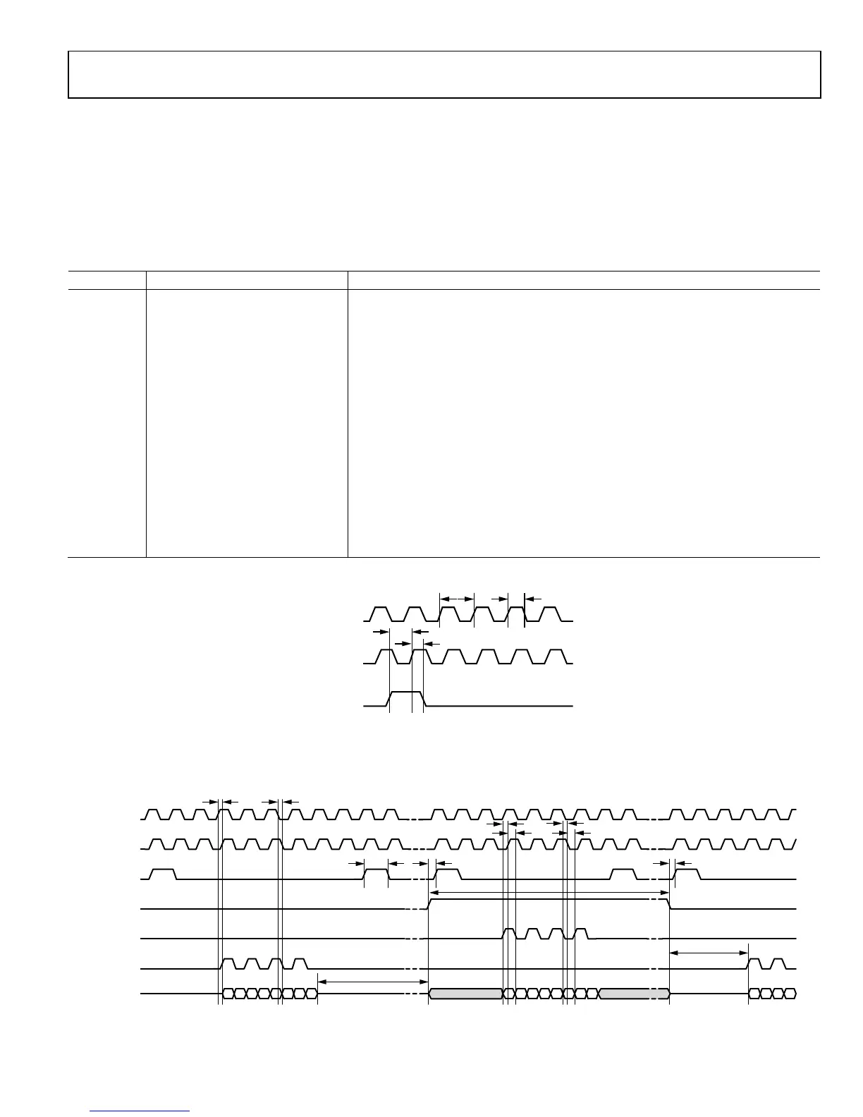
DATA PATH TIMING PARAMETERS (CMOS)
The timing parameters in Table 49 are listed to provide
guidance when interfacing the AD9361 to a BBP. Figure 76
shows the relationship between the data clocks and the
hardware control inputs. Figure 77 show the relationship
among all other parameters.
Table 49. Data Path Timing Constraint Values
Parameter Min Typical Max Description
t
CP
16.276 ns DATA_CLK cycle time (clock period)
t
MP
45% of t
CP
55% of t
CP
DATA_CLK and FB_CLK high and/or low minimum pulse width
(including effects of duty cycle distortion, period jitter, cycle-cycle jitter and half-
period jitter)
t
SC
1 ns Control signal setup time to FB_CLK at AD9361 inputs (ENABLE, TXNRX)
t
HC
0 ns Control signal hold time from FB_CLK at AD9361 inputs (ENABLE, TXNRX)
t
STx
1 ns Tx data setup time to FB_CLK at AD9361 inputs
t
HTx
0 ns Tx data hold time from FB_CLK at AD9361 inputs
t
DDRx
0 ns 1.5 ns
1.2 ns
Rx data delay from DATA_CLK to D[11:0] outputs – 1.8 V supply
Rx data delay from DATA_CLK to D[11:0] outputs – 2.5 V supply
t
DDDV
0 ns 1.0 ns Rx data delay from DATA_CLK to Rx_FRAME
t
ENPW
t
CP
ENABLE pulse width (edge-detected by FB_CLK)
t
TXNRXPW
t
CP
TXNRX pulse width (edge-detected by FB_CLK)
t
TXNRXSU
0 ns TXNRX setup time to ENABLE
t
RPRE
2 × t
CP
Time at which BBP stops driving D[11:0] before a receive burst, TDD
t
RPST
2 × t
CP
Time at which BBP starts driving D[11:0] after a receive burst, TDD
Figure 7
6. Data Port Timing Parameter Diagrams – Data Reference Clocks and Hardware Control Inputs (CMOS Bus Configuration)
Figure 7
7. Data Port Timing Parameter Diagrams – CMOS Bus Configuration (Example shown is Single Port, DDR, TDD Operation)
DATA_CLK_P
FB_CLK_P
ENABLE
1
1
THE SAME TIMING RULES APPLY TO TXNRX.
t
CP
t
MP
t
HC
t
SC
11668-077
P0_D[11:0]
TXNRX
ENABLE
DAT
_CLK_P
FB_CLK_P
TX_FRAME
RX_FRAME
RI RQ RI RI RIRQ RQ RQ TQ TI TQ TI TQ TI TQ RI RQ RI RQTI
t
DDRX,
t
DDDV
t
RPST
t
DDRX,
t
DDDV
t
TXNRXSU
t
ENPW
t
TXNRXSU
t
RPRE
t
TXNRXPW
t
HTX
t
HTX
t
STX
t
STX
11668-078

 Loading...


