EasyManua.ls Logo

Analog Devices AD9361 User Manual

Analog Devices AD9361
128 pages
To Next Page IconTo Next Page
To Previous Page IconTo Previous Page
Page #36 background imageLoading...
Page #36 background image
UG-570 AD9361 Reference Manual
| Page 36 of 128
GAIN CONTROL THRESHOLD DETECTORS
The AD9361 uses detectors to determine if the received signal is
overloading a particular block or if the signal has dropped below
programmable thresholds. LMT and ADC overload detectors
(also referred to as peak detectors) react to nearly instantaneous
overload events. In contrast, a power measurement in the
AD9361 occurs over 16 or more Rx samples. Figure 18 shows
where these detectors are located in signal path.
LMT OVERLOAD DETECTOR
The LNA/mixer/transimpedance amplifier (LMT) overload
detector is an analog peak detector used to determine if the
received signal is overloading the blocks before the analog low-
pass filter. If an LMT overload occurs but the ADC does not
overload, it may indicate that an out-of-band interfering signal is
resulting in the overload condition.
There are two different LMT overload thresholds, one used to
indicate larger overloads and one used to indicate smaller
overloads. Both thresholds are programmable and are configured
in the ad9361_set_rx_gain_control_mode function. The small
threshold should be set such that it is lower than (or equal to)
the large threshold since the AGC will be affected differently
depending on which threshold is exceeded. In MGC mode, the
BBP can monitor the overload flags via the control output pins.
Equation 15 describes both large and small thresholds.

󰇛

󰇜
16mV
󰇛󰇟5:0󰇠 1󰇜
(15)
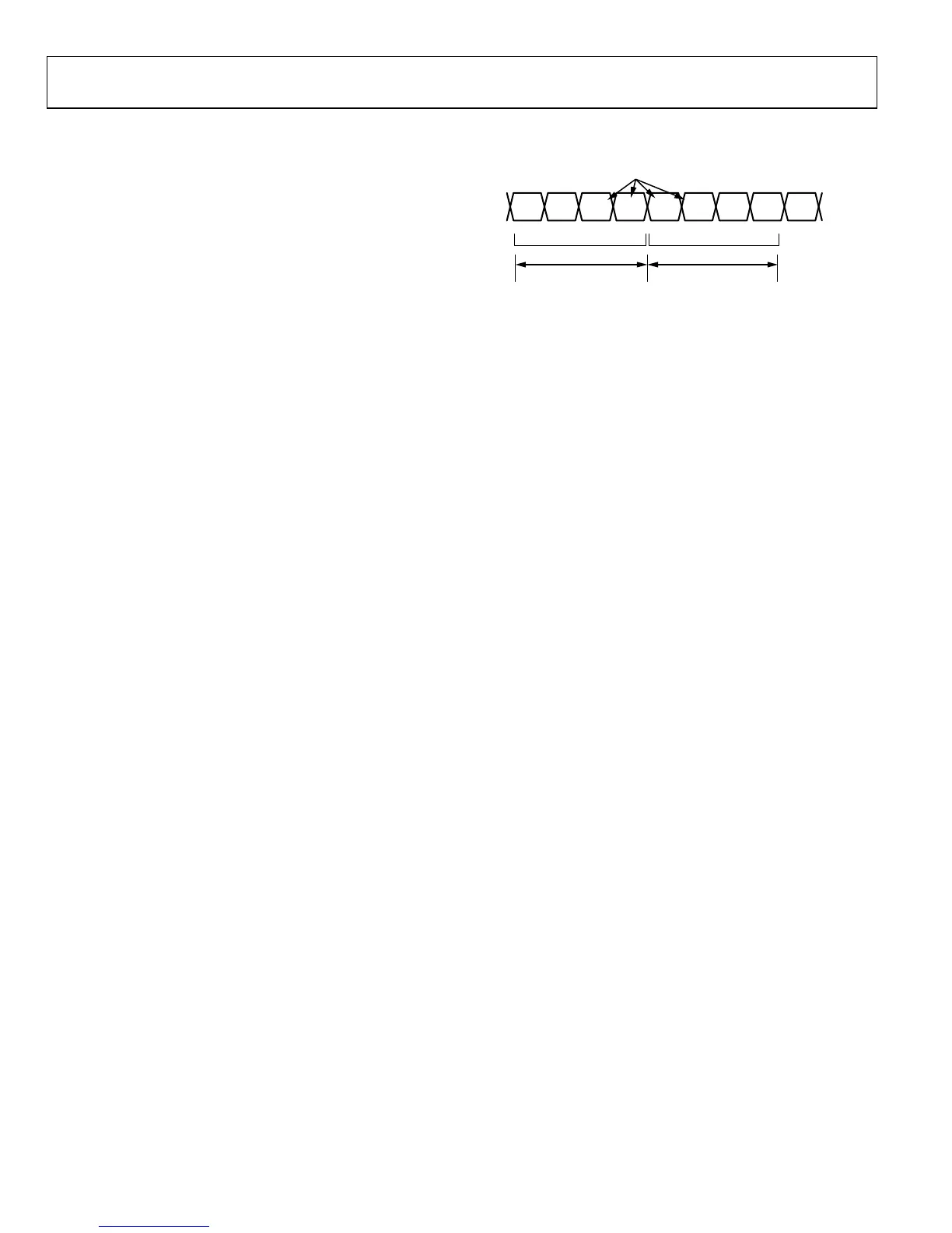
ADC OVERLOAD DETECTOR
The ADC is a highly oversampled sigma-delta modulator (SDM)
with an output ranging from +4 to −4. A particular ADC output
sample does not necessarily represent the input signal at a
particular time. Rather, a positive value indicates that the input
signal is more positive since the last sample and a negative value
indicates that the input signal is more negative since the last
sample. Note that since the ADC is highly oversampled, the ADC
clock is much faster than the receive sample rate. Decimating and
low-pass filtering result in digital samples that represent the
analog signal.
When the ADC is overloaded, the error between its samples and
the input signal will cause the ADC to output more samples with
values of +4 or −4 as it struggles to track the input signal.
Figure 20 shows how the ADC overload detector processes
signals and how the thresholds are used.
Figure 20. ADC Over Range Detection Algorithm
There are two programmable thresholds, both of which are
configured in the ad9361_set_rx_gain_control_mode function.
The thresholds are common to both receivers. The number of
samples to use in the sum-of-squares calculation is also set in the
ad9361_set_rx_gain_control_mode function. The resulting value,
z, shown in the Figure 20 is compared against the two thresholds
and if a particular threshold is exceeded, a flag is set. In MGC
mode, the BBP can monitor the overload flag(s) via the control
output pins.
LOW POWER THRESHOLD
The low power threshold is an absolute threshold measured in
−dBFS with a resolution of 0.5 dBFS per LSB. The range is from
0 dBFS to −63.5 dBFS. The value is programmed with the
ad9361_set_rx_gain_control_mode function. The AD9361 uses
this threshold in the fast attack AGC mode and it can also be used
in MGC mode, both of which are described later in the Fast
Attack AGC Mode section and MGC Overview section. In fast
attack AGC mode, the low power flag does not assert immediately
after the average signal power drops below the low power
threshold. The flag only asserts once the signal power has
remained below the low power Threshold for a time equal to the
increment time. The increment time value is measured in ClkRF
cycles (the clock used at the input of the receive FIR filter). In
MGC mode, the increment time value is not used and the low
power flag asserts as soon as the power drops below the low
power threshold.
AVERAGE SIGNAL POWER
When measuring power (such as for low power threshold), the
measurement is an average of a certain number of samples set by
the decimated power measurement duration, which is set in the
ad9361_set_rx_gain_control_mode function. The duration is
common to both receivers. At the end of each measurement
period, the average signal power value updates. The actual
duration in Rx sample periods is per Equation 16.
abcdabcd
a
2
+ ++ +++
= z = z
A
DC SAMPLE VALUES
b
2
c
2
d
2
a
2
b
2
c
2
d
2
11668-021
Rev. A

Table of Contents

Question and Answer IconNeed help?

Do you have a question about the Analog Devices AD9361 and is the answer not in the manual?

Analog Devices AD9361 Specifications

General IconGeneral
BrandAnalog Devices
ModelAD9361
CategoryMotherboard
LanguageEnglish

Summary

General Information

AD9361 Registers and Driver Support

Information about AD9361 registers and driver availability.

AD9361 Driver Support Resources

Support resources for AD9361 drivers.

Introduction and Terminology

Key Terminology Definitions

Definitions of key terms used in the manual.

Register and Bit Syntax Conventions

Format for describing registers and bits.

Initialization and Calibration Procedures

BBPLL VCO Calibration

Calibration of the Baseband PLL VCO.

RF Synthesizer Charge Pump Calibration

Calibration of RF PLL charge pump currents.

RF Synthesizer VCO Calibration

Calibration of RF PLL VCOs.

Baseband Rx Analog Filter Tuning

Tuning the Rx anti-aliasing filter.

Baseband Tx Analog Filter Tuning

Tuning the Tx anti-imaging filter.

Baseband Tx Secondary Filter Programming

Programming the Tx secondary filter.

Rx TIA Calibration Equations

Calibration of the Rx transimpedance amplifier.

Rx ADC Setup Configuration

Configuration for the receive ADC.

Baseband DC Offset Calibration

Calibrating baseband DC offset.

Baseband DC Offset Tracking

Tracking baseband DC offset.

RF DC Offset Calibration

Calibrating RF DC offset.

Rx Quadrature Tracking Calibration

Minimizing Rx phase and gain error.

Tx Quadrature Calibration

Minimizing Tx DC offset, gain, and phase errors.

Reference Clock Requirements and Setup

DCXO Setup and Operation

Setting up and operating the Digitally Controlled Crystal Oscillator.

Reference Clock Setup and Operation

Setting up and operating the reference clock.

Phase Noise Specification

Phase noise requirements for the clock source.

RF and Baseband PLL Synthesizer

AD9361 PLL Architecture Overview

Block diagrams of the AD9361 PLL.

PLL Reference Block Details

Details of the reference block in the PLL architecture.

Main PLL Block Description

The independent Rx and Tx PLL blocks.

Synthesizer Configuration and Control

Charge Pump Current Configuration

Configuring the charge pump current.

RFPLL Loop Filter Details

Details of the RFPLL loop filter.

VCO Configuration

Configuring the Voltage Controlled Oscillator.

VCO Calibration Process

Process for calibrating the VCO.

VCO Vtune Measurement

Measuring the VCO Vtune voltage.

Lock Detector Configuration

Configuring the lock detector.

Fast Lock Profiles and Pin Select

Fast Lock Profiles Overview

Storing synthesizer programming information for faster frequency changes.

Fast Lock Initial Wider Bandwidth Option

Using wider loop bandwidth for faster lock times.

Fast Lock Pin Select Functionality

Selecting fast lock profiles using hardware control pins.

Enable State Machine Guide

Enable State Machine (ENSM) Overview

Real-time control of device state using the ENSM.

ENSM State Definitions

Definitions of ENSM states.

ENSM Modes of Operation

Controlling the ENSM via SPI or pins.

SPI Control for ENSM

Controlling the ENSM via SPI.

Sleep State Management

Entering and Exiting Sleep State

Steps to enter and exit the sleep state.

Calibrations After Waking from Sleep

Recalibrations needed after waking from sleep.

Filter Guide and Signal Paths

Transmit Signal Path Description

Description of the AD9361 transmit signal path.

Transmit Digital Filter Blocks

Details of digital filters in the Tx path.

Transmit FIR Filter Details

Description of the transmit FIR filter.

Receive Signal Path Description

Description of the AD9361 receive signal path.

Receive Analog Filter Blocks

Analog filters before the ADC in the Rx path.

Rx TIA LPF Filter

Rx Transimpedance Amplifier Low-Pass Filter.

Rx BB LPF Filter

Rx Baseband Low-Pass Filter.

Receive Digital Filter Blocks

Digital filters after the ADC in the Rx path.

Rx HB3/DEC3 Filter

Rx HB3/DEC3 decimating filter.

Rx HB2 Filter

Rx HB2 decimating filter.

Rx HB1 Filter

Rx HB1 decimating filter.

Receive FIR Filter Details

Description of the receive FIR filter.

Digital Rx Block Delay Calculation

Calculation of digital Rx block delay.

Gain Control Mechanisms

Gain Table Overview

Overview of gain tables and pointers.

Full Table Mode Configuration

Using a single gain table for all receiver blocks.

Split Table Mode Configuration

Splitting gain tables for improved noise figure.

Digital Gain Implementation

Adding digital gain to the system.

Manual Gain Control (MGC) Overview

Manual Gain Control overview.

Automatic Gain Control (AGC) Modes

Slow Attack AGC Mode

AGC mode for slowly changing signals.

Slow Attack AGC Gain Update Time

Timing for AGC gain updates in slow attack mode.

Hybrid AGC Mode Operation

Hybrid AGC mode operation.

Fast Attack AGC Mode Operation

Fast attack AGC mode operation.

Fast Attack AGC State Machine

State 0: Reset

Initial reset state of the AGC.

State 1: Peak Overload Detect

Detecting peak overloads and adjusting gain.

State 2: Measure Power and Lock Level Gain Change

Measuring power and changing gain to lock level.

State 3: Measure Power and Peak Overload Detect

Measuring power and detecting peak overloads.

State 4: Unlock Gain

Reducing gain and unlocking the AGC.

State 5: Gain Lock and Measure Power

Locking gain and measuring average power.

Custom Gain Table Configuration

Custom Gain Tables Overview

Overview of modifying gain tables for optimal RF performance.

LNA Gain vs. Index Mapping

LNA gain settings based on index.

Mixer Gm Gain vs. Index Mapping

Mixer gain settings based on index.

TIA Gain vs. Index Mapping

TIA gain settings based on index.

LPF Index vs. Gain Mapping

LPF gain settings based on index.

Digital Index vs. Digital Gain Mapping

Digital gain settings based on index.

RF DC Calibration Bit and Table Index

RF DC Calibration Bit Functionality

Functionality of the RF DC Calibration bit.

Maximum Full Table/LMT Table Index

Setting the maximum index for gain tables.

External LNA Integration

Integrating external LNAs with the AD9361.

Received Signal Strength Indicator (RSSI)

RSSI Mode Select and Measurement Duration

Selecting RSSI mode and measurement duration.

RSSI Weighting Calculation

Weighting RSSI measurements.

RSSI Delay and RSSI Wait Settings

RSSI delay and wait settings.

RSSI RFIR Configuration

Configuring the RFIR for RSSI measurements.

RSSI Gain Step Calibration

Calibrating RSSI gain steps.

Transmit Power Control (TPC)

Transmit Power Control Overview

Overview of transmit power control.

Tx Attenuation Words

Controls attenuation of the transmit path.

Attenuation Word Update Options

Options for implementing attenuation words.

Tx Power Monitor (TPM) Operation

Tx Power Monitor Overview

Overview of the Tx power monitor circuit.

Tx Power Monitor Description

Description of the Tx power monitor circuit.

Input Matching/Attenuation Network

Matching network for TPM inputs.

Tx Power Monitor Gain Control

Gain control for the Tx power monitor.

TPM Dynamic Range and Test Modes

TPM Dynamic Range Maximization

Maximizing TPM dynamic range.

Example TxMON Configuration

Example TxMON configuration for TPM transfer function.

TPM Test Mode

Using TPM test mode for data output.

RF Port Interface Guidelines

RF Port Interface Overview

Defining expected AD9361 port impedance values.

Rx Interface Considerations

Considerations for Rx interface configuration.

Interfacing with External Components

Interfacing with external components.

Rx LNA Maximum Input Power

Maximum input power for Rx LNA.

Rx LNA Input Port DC Voltage

DC voltage level for Rx LNA input.

Tx Output Port Bias

Bias voltage for Tx output ports.

Board Design Considerations

Considerations for board layout and matching.

Rx Signal Path Interface Circuits

Single-ended and differential interface circuits.

Factory Calibration Procedures

Factory Calibration Overview

Overview of necessary factory calibrations.

Internal DCXO Calibration

Digitally Controlled Crystal Oscillator setup.

Tx RSSI (Tx Monitor) Calibration

Transmit RSSI measurement calibration.

Rx RSSI Calibration

Receive RSSI measurement calibration.

Rx GM/LNA Gain Step Calibration

Calibrating Rx GM/LNA gain steps.

Tx Power Out vs. Tx Attenuation Calibration

Calibration for Tx power output.

Control Output Signals

Control Output Bit Descriptions

Description of control output bits.

Control Output Table Mapping

Mapping of control outputs to signals.

Control Output Signal Descriptions

Detailed description of control output signals.

0x035 = 0x00: Calibration Busy and Done

Control output for calibration status.

0x035 = 0x01: PLL Lock Status

Control output for PLL lock status.

0x035 = 0x02: Calibration Busy Status

Control output for calibration busy status.

0x035 = 0x03: Rx Gain Control Outputs

Control outputs for Rx gain control.

0x035 = 0x09: RxON, TxON, RSSI Signals

Control signals for Rx/Tx enable and RSSI status.

0x035 = 0x0A: Digital Overflow Status

Control output for digital overflow status.

0x035 = 0x0B: Calibration and ENSM States

Control outputs for calibration and ENSM states.

0x035 = 0x0C: Gain Control Outputs

Control outputs related to gain control.

0x035 = 0x0D: Tx Quadrature and RF DC Calibration Status

Status of Tx quadrature and RF DC calibration.

0x035 = 0x0E: Rx Quadrature and BB DC Calibration Status

Status of Rx quadrature and BB DC calibration.

0x035 = 0x0F: Gain Control Outputs

Control outputs for gain control.

0x035 = 0x10: Gain Control and RSSI Signals

Control signals for gain control and RSSI.

0x035 = 0x11: AuxADC Digital Output

AuxADC digital output data.

0x035 = 0x12: Gain Control, Power Word Ready

Control signals for gain control and power word ready.

0x035 = 0x13: Gain Control, Power Word Ready

Control signals for gain control and power word ready.

0x035 = 0x14: Digital Overflow Status

Control output for digital overflow status.

0x035 = 0x15: DC Offset Tracking

Control signals for DC offset tracking.

0x035 = 0x16: Gain Control Outputs

Control outputs for gain control.

0x035 = 0x17: Gain Control Outputs

Control outputs for gain control.

0x035 = 0x18: DC Offset Tracking, Power Word Ready

Control signals for DC offset tracking and power word ready.

0x035 = 0x19: Charge Pump Calibration States

Control outputs for charge pump calibration states.

0x035 = 0x1A: Rx VCO and ALC Calibration States

Control outputs for Rx VCO and ALC calibration states.

0x035 = 0x1B: Tx VCO and ALC Calibration States

Control outputs for Tx VCO and ALC calibration states.

0x035 = 0x1C: Rx VCO Calibration States

Control outputs for Rx VCO calibration states.

0x035 = 0x1D: Tx VCO Calibration States

Control outputs for Tx VCO calibration states.

0x035 = 0x1E: Gain Control, Temp Sense Valid, AuxADC Valid

Control signals for gain, temp sense, and AuxADC validity.

0x035 = 0x1F: Gain Control Outputs

Control outputs for gain control.

Auxiliary Features: DAC, ADC, GPO, Temp Sensor

Auxiliary DAC (AuxDAC) Description

Description of auxiliary DACs.

Auxiliary ADC (AuxADC) Description

Description of auxiliary ADC.

Internal Temperature Sensor Measurement

Measuring the internal temperature sensor.

General Purpose Output (GPO) Control

Controlling the general-purpose output pins.

GPO Auto Toggle Functionality

Automatic GPO toggling based on ENSM.

Synchronization Procedures

Baseband Synchronization Overview

Overview of baseband synchronization.

Multichip Synchronization

Synchronizing multiple AD9361 devices.

Multichip Synchronization Procedure

Procedure for synchronizing multiple devices.

Synchronization Verification Methods

Methods for verifying data synchronization.

Digital Interface Specifications

Digital Interface Overview

Overview of digital interfaces.

CMOS Mode Interface Characteristics

CMOS mode interface characteristics.

LVDS Mode Interface Characteristics

LVDS mode interface characteristics.

CMOS Mode Data Path and Clock Signals

Description of CMOS data path and clock signals.

P0_D and P1_D Data Ports

Description of parallel data ports.

DATA_CLK Signal

Receive data path master clock.

FB_CLK Signal

Feedback clock for transmit data.

RX_FRAME Signal

Frame signal for receive data.

TX_FRAME Signal

Frame signal for transmit data.

ENABLE Signal for Burst Control

Signal for controlling data transfer bursts.

TXNRX Signal for Direction Control

Signal for controlling data transfer direction.

CMOS Clock Rates and Signal Bandwidths

Maximum clock rates and signal bandwidths in CMOS mode.

Single Port Half Duplex Mode (CMOS)

Mode for TDD operation and data rates < 61.44 MHz.

Single Port TDD Functional Timing (CMOS)

Timing diagrams for single port TDD mode.

Single Port Full Duplex Mode (CMOS)

Mode for FDD operation and data rates < 30.72 MHz.

Dual Port Half Duplex Mode (CMOS)

Mode for TDD operation and data rates up to 122.88 MHz.

Dual Port Full Duplex Mode (LVDS)

Mode for FDD operation and data rates < 61.44 MHz.

Data Path Functional Timing (LVDS)

Timing diagrams for dual port FDD LVDS mode.

Data Path Timing Parameters (LVDS)

Timing constraints for LVDS data buses.

Serial Peripheral Interface (SPI)

SPI Interface Overview

Mechanism for digital control of the AD9361.

SPI Functional Layer Configuration

Configuration of the SPI interface.

SPI Data Transfer Protocol

Protocol for SPI data transfers.

Phase 1 Instruction Format

Format of the SPI instruction word.

Additional Interface Signals

CLOCK_OUT Signal

Output clock signal for the BBP.

CTRL_IN Input Pins

Programmable input signals for real-time control.

CTRL_OUT Output Signals

Programmable output signals for status.

EN_AGC Input Signal

Input signal for real-time AGC control.

GPO Output Pins

General-purpose output pins.

RESETB Hardware Reset Input

Hardware reset input signal.

SYNC_IN Synchronization Input

Synchronization input for multiple devices.

Power Supply and Layout Guidelines

PCB Material and Stack Up Selection

Guidelines for PCB material and stack-up.

RF Transmission Line Layout

Guidelines for routing RF transmission lines.

Fan-Out and Trace Space Guidelines

Guidelines for BGA fan-out and trace spacing.

Component Placement and Routing

Component Placement and Routing Guidelines

Guidelines for placing critical components and signals.

Power Management and System Noise Considerations

Analysis of power supply noise effects on performance.

Power Supply Options Analysis

1.3V Analog Supply with LDO

Using an LDO for the 1.3V analog supply.

1.3V Analog Supply with Switching Regulator

Using a switching regulator for the 1.3V analog supply.

Effects of Power Supply Noise on Phase Noise

Analysis of power supply noise effects on phase noise.

Power Supply Distributions

Power Supply Balls and Recommendations

Power supply ball assignments and routing.

Rx LO Frequency Deviations Due to Power Supply Transients

Related product manuals