UG-570 AD9361 Reference Manual
| Page 90 of 128
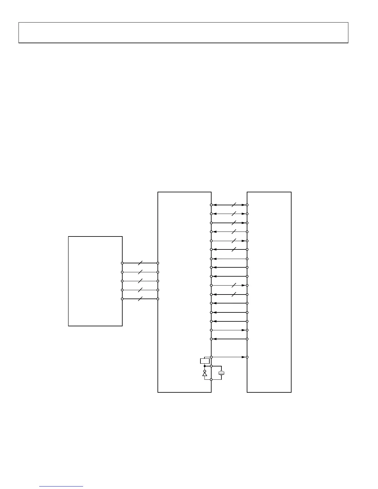
DIGITAL INTERFACE SPECIFICATION
OVERVIEW
This section defines the parallel data ports and the serial
peripheral interface (SPI) that enable the transfer of data and
control/status information between the AD9361 and a BBP.
Figure 63 illustrates these interfaces as well as provides a high-
level view of how the AD9361 and BBP are used in a broadband
wireless system. The data interface operates in one of two
modes: standard CMOS compatible mode or low-voltage
differential signal (LVDS) compatible mode. Each interface
possesses unique characteristics described in the following
sections.
When CMOS mode is used:
• Single ended-CMOS logic compatibility is maintained.
• Either one or both data ports may be utilized. Using two
ports allows for higher data throughput.
• Both frequency-division duplex (FDD) and time-division
duplex (TDD) operation are supported with one data port
or two.
When LVDS mode is used:
• Data port signaling is differential LVDS, allowing up to
12-inch PCB traces/connector interconnects between the
AD9361 and the BBP.
• Only the data port (including clocking and other
associated timing signals) is LVDS compatible.
• Both FDD and TDD operation are supported.
Fig
ure 63. AD9361 Interface
2
8
12
2
4
12
P1_D[11:0]
12
P0_D[11:0]
2
DATA_CLK
2
FB_CLK
2
RX_FRAME
2
TX_FRAME
TXNRX
ENABLE
EN_AGC
8
CTRL_OUT
4
CTRL_IN
SPI_ENB
SPI_CLK
SPI_DI
SPI_DO
SYNC_IN
XTAL_N
AD9361
RF
FRONT END
BBP
AUX_DAC
TX
RX
TX_MON
GPO
CLK_OUT
XTAL_P
PLL
11668-064

 Loading...


