AD9361 Reference Manual UG-570
| Page 93 of 128
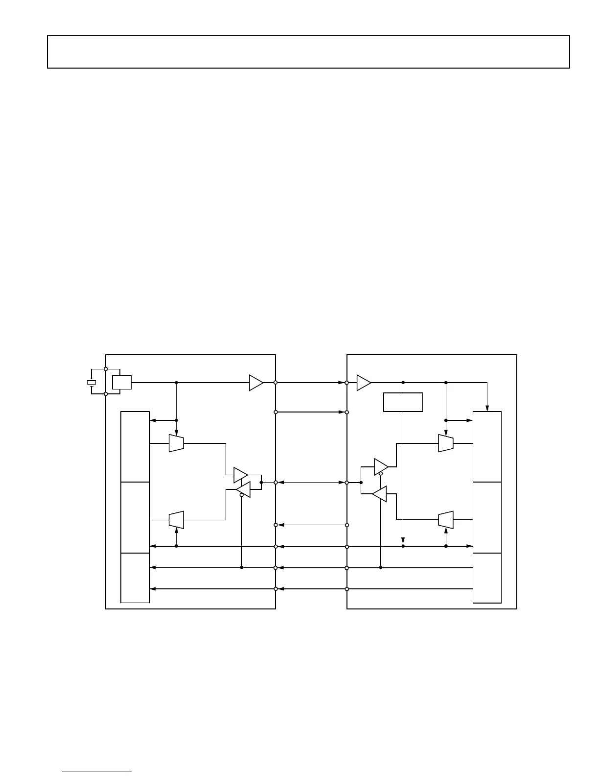
SINGLE PORT HALF DUPLEX MODE (CMOS)
Single port half duplex mode is used in applications requiring
TDD operation and data rates less than 61.44 MHz. In this
mode, the bus is utilized in a bidirectional manner so that data
can be received or transmitted on the same lines. This mode can
be used with all receiver-transmitter configurations (1R1T,
2R1T, 1R2T, and 2R2T) and is typically employed when there is
limited PCB space or the BBP has only a single data bus port
available. The bus can be operated as either single data rate
(SDR) or dual data rate (DDR) in this configuration. In this
mode, the enabled port is multiplexed between transmit and
receive operation while the unused port is disabled. The
enabled port is determined by the Swap Ports bit in SPI register
0x012. Figure 64 illustrates the connections between the
AD9361 and the BBP for this mode of operation.
During an Rx burst, D[11:0] is driven by the AD9361 such that
the setup and hold times between DATA_CLK and D[11:0]
arriving allow the BBP to use DATA_CLK to capture the data.
Similarly, during a Tx burst, D[11:0] is driven by the BBP such
that the setup and hold times between FB_CLK and D[11:0]
allow the AD9361 to use FB_CLK to capture the data. A data
transfer starts when the ENABLE signal pulses (or goes high),
and the end of the data transfer is marked but another pulse on
the ENABLE line (or when it returns low). The direction of data
transfer is determined by the TXNRX signal. When this signal
is low and the ENSM is in the Rx or FDD state, the bus is
configured in the receive direction (data transferred from
AD9361 to BBP). When TXNRX is driven high and the ENSM
has moved out of the Rx or FDD state, the ENSM changes the
bus to the transmit direction (data transferred from BBP to
AD9361).
The Rx_FRAME and Tx_FRAME signals indicate the
beginning of a set (frame) of data samples. The Rx_FRAME
can be set to occur once at the beginning of the burst (one high
transition only) for each data transfer or to have a rising edge at
the beginning of each frame and repeat with a 50% duty cycle
until the data transfer is complete. Similarly, Tx_FRAME
accepts either format from the BBP.
During a transmit burst, the BBP drives the data values on
P0_D[11:0] using FB_CLK and Tx_FRAME. During a Rx
burst, the AD9361 drives the data values on P0_D[11:0] using
DATA_CLK and Rx_FRAME.
Fig
ure 64. Single Port TDD Mode Bus Configuration
DATA_CLK
RX_FRAME
P0_D[11:0]
TX_FRAME
FB_CLK
TXNRX
ENABLE
RX
DATA
RX
DATA
TX
DATA
TX
DATA
CTRL CTRL
PLL
FEEDBACK
CLK GEN
AD9361
BBP
11668-065

 Loading...


