UG-570 AD9361 Reference Manual
| Page 14 of 128
REFERENCE CLOCK REQUIREMENTS
OVERVIEW
The AD9361 uses fractional-n phase locked loops (PLLs) to
generate the transmitter and receiver local oscillator (LO)
frequencies as well as the oscillator (the baseband PLL) used for
the data converters, digital filters, and I/O port. These PLLs all
require a reference clock input, which can be provided by an
external oscillator or by an external crystal (XO) and a digitally
programmable on-chip variable capacitor. The capacitor fine-
tunes the resulting reference clock frequency. This combination
of XO and trimming capacitor is collectively referred to as the
DCXO.
Applications such as wireless base stations require that the
reference clock lock to a system master clock. In these
situations, use an external oscillator such as a VCTCXO in
conjunction with a synchronizing PLL such as the AD9548.
Wireless user equipment (UE), however, dos not typically need
to be locked to a master clock but they do need to adjust the LO
frequency periodically to maintain connection with a base
station. The base station (BTS) occasionally informs the UE of
its frequency error relative to the BTS. By adjusting the
trimming capacitor, the baseband processor can adjust the
reference clock frequency and thus the LO frequency as needed.
The RFPLLs and the BBPLL should maintain minimal
frequency drift with temperature. However, typical XOs have an
S curve response of frequency vs. temperature, making it more
difficult for a baseband processor to correct the frequency error
at startup and during operation.
This section describes the setup, operation, and recommended
specification of the DCXO and reference clock.
DCXO SETUP AND OPERATION
To use the DCXO, connect an external crystal (XO) between the
XTALP and XTALN pins of the AD9361. Valid crystal resonant
frequencies range from 19 MHz to 50 MHz. The crystal must be
an AT cut fundamental mode of vibration with a load
capacitance of 10 pF.
By adjusting a capacitor within the AD9361, the resulting
DCXO frequency can be adjusted to compensate for XO
frequency tolerance and stability. This adjustment is enabled
using the ad9361_set_dcxo_tune function. The resolution of the
DCXO varies with coarse word with a worst-case resolution (at
coarse word = 0) of 0.0125 ppm. Using both coarse and fine
words, the DCXO can vary the frequency over a ±60 ppm
range.
Using a bench test, nominal DCXO trimming words should be
determined and then used in during initialization. These
nominal words should be written before the BBPLL is
calibrated. After initialization (after the BBPLL and RFPLLs are
programmed, calibrated, and locked), the DCXO words may be
written at any time.
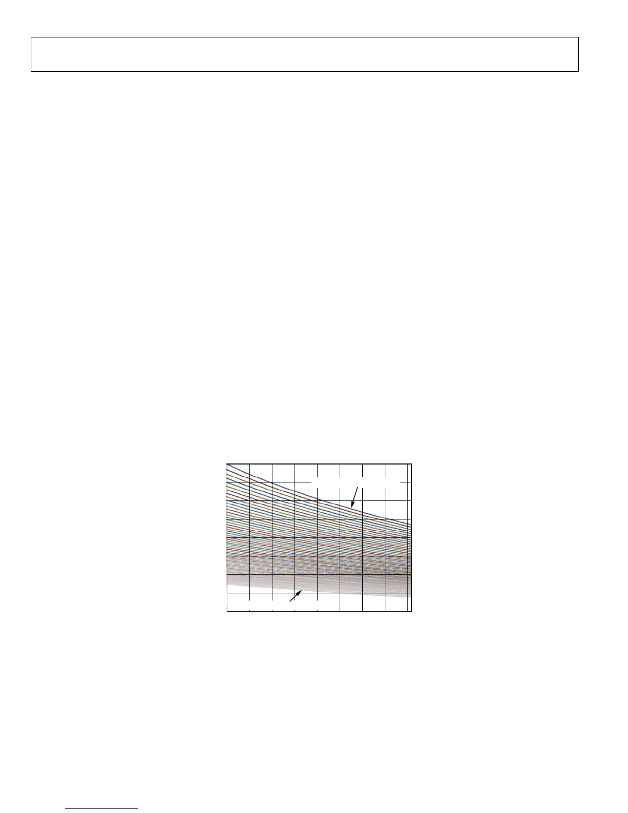
Figure 1 shows the variation of DCXO frequency over all
possible variations of coarse and fine word. The XO nominal
frequency used in this test was 40 MHz.
Fig
ure 1. DCXO Frequency vs. Coarse and Fine Words
40003000
39995000
39996000
39997000
39998000
39999000
40000000
40001000
40002000
0 1000 2000 3000 4000 5000 6000 7000 8000
DCXO FREQUENCY (Hz)
DCXO FINE WORD (REG 0x293 AND 0x294)
COARSE WORD IN 0x292 = 63
COARSE WORD IN 0x292 = 0
11668-002

 Loading...


