AD9361 Reference Manual UG-570
| Page 87 of 128
BASEBAND SYNCHRONIZATION
OVERVIEW
For broadband wireless access (BWA) systems, multi input-
multi output (MIMO) operation and RF beamforming are
proven techniques for maximizing throughput and efficient
spectrum utilization. Modern integrated devices with
multichannel Rx and multichannel Tx capability such as the
AD9361 make developing MIMO systems with high
performance and linearity utilizing integrated receivers,
transmitters, and synthesizers a simpler task.
Some systems may require more complex configurations that
combine multiple devices. Operating multiple devices while
trying to coordinate data for each channel of each device is not
practical for devices that operate independently without any
mechanism for aligning data timing. Data synchronization into
and out of multiple devices is required to implement such
configurations successfully.
The AD9361 is capable of providing the synchronization
necessary to implement multichannel systems. This device
contains the external control inputs and internal circuitry
needed to synchronize baseband sampling and data clocks,
allowing the system design to utilize multiple devices in parallel
with equivalent performance to a single device.
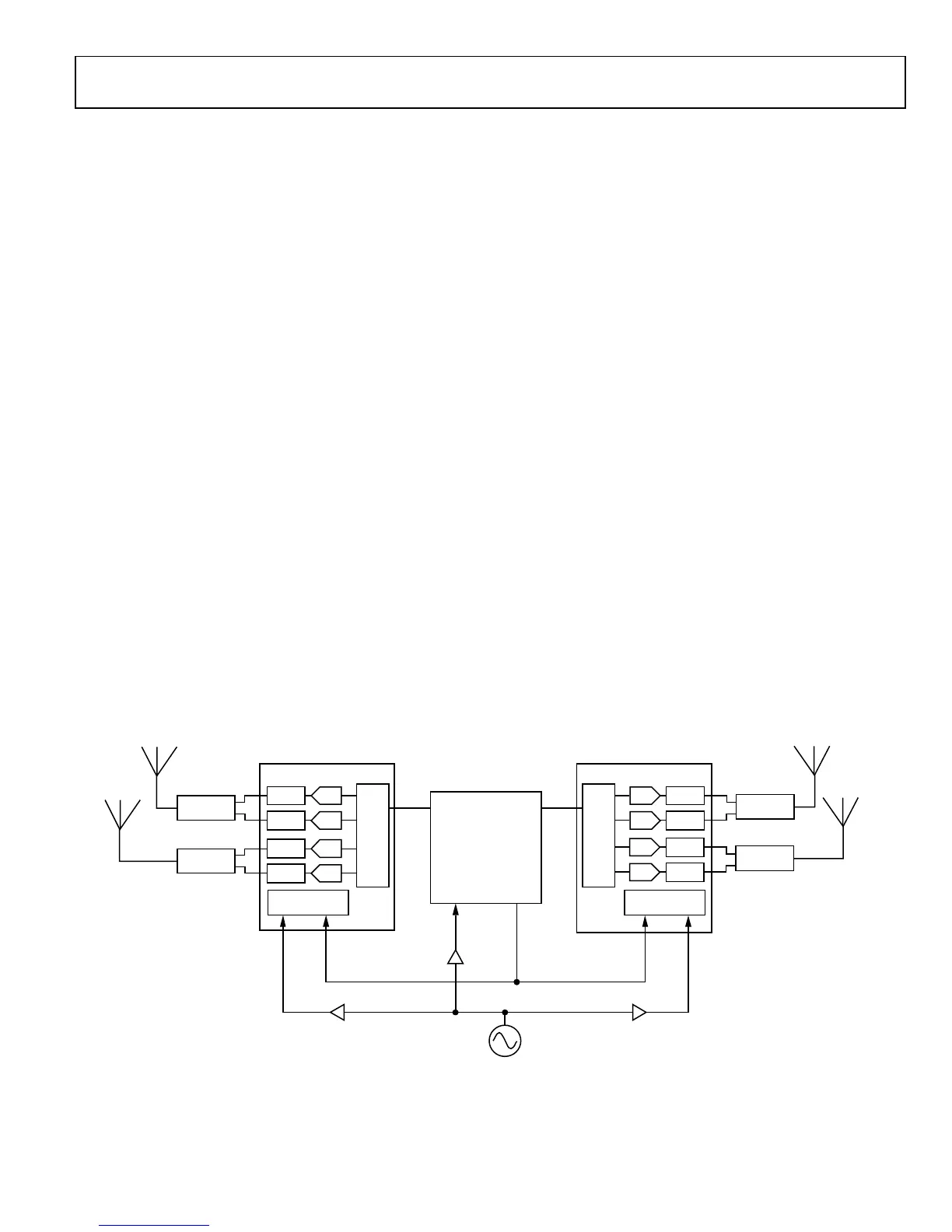
MULTICHIP SYNCHRONIZATION
The device utilizes a fractional-N synthesizer in the baseband
PLL block to generate the desired sample rate for the system.
This synthesizer generates the ADC sample clock, DAC sample
clock, and baseband digital clocks from any reference clock in
the frequency range specified for the reference clock input. For
MIMO systems requiring more than two input or two output
channels, multiple AD9361 devices and a common reference
oscillator are required. The AD9361 provides the capability to
accept an external reference clock and synchronize operation
with other devices using simple control logic. Each AD9361
includes its own baseband PLL that generates sampling and data
clocks from the reference clock input, so an additional control
mechanism is required to synchronize multiple devices. A
logical SYNC_IN pulse input is needed to align each device’s
data clock with a common reference. Figure 59 illustrates the
connections necessary to synchronize two AD9361 devices. The
oscillator output is buffered into each device using an ADA4851-4
quad high-speed op amp as a clock buffer amplifier. Another
alternative is to use a clock buffer IC like the AD9548 to
distribute a buffered clock to each device while minimizing the
noise coupling between devices. The procedure following
Figure 59 explains how to synchronize two devices, but it
should be noted that additional devices could be connected in
parallel using this procedure. The total number of devices that
can be connected in parallel is limited only by the drive
capability of the clock and logic signals.
Note that this function does not include RF synchronization.
The ability to synchronize RF local oscillators is not available
with this device. Baseband PLL synchronization is the only
alignment among multiple chips that is possible using this
feature. If the MCS RF Enable bit is set then the RF LO dividers
will remain enabled in the alert state. This will allow for the RF
phase relationship between multiple devices to remain constant
throughout operation.
Fig
ure 59. BB Multichip Synchronization Configuration
DUPLEXER
DUPLEXER
TX1
RX1
TX1
RX1
DAC DAC
ADC
ADC
BB
I/F
BB
I/F
BASEBAND
PROCESSOR
REFERENCE
OCILLATOR
ADA4851-4 ADA4851-4
ADA4851-4
BBPLL
BBPLL
XTALN
XTALN
SYNC_IN
SYNC_IN
SYS
CLK
BB
SYNC
11668-060
DUPLEXER
TX2
RX2
DAC
ADC
DUPLEXER
TX2
RX2
DAC
ADC

 Loading...


