UG-570 AD9361 Reference Manual
| Page 86 of 128
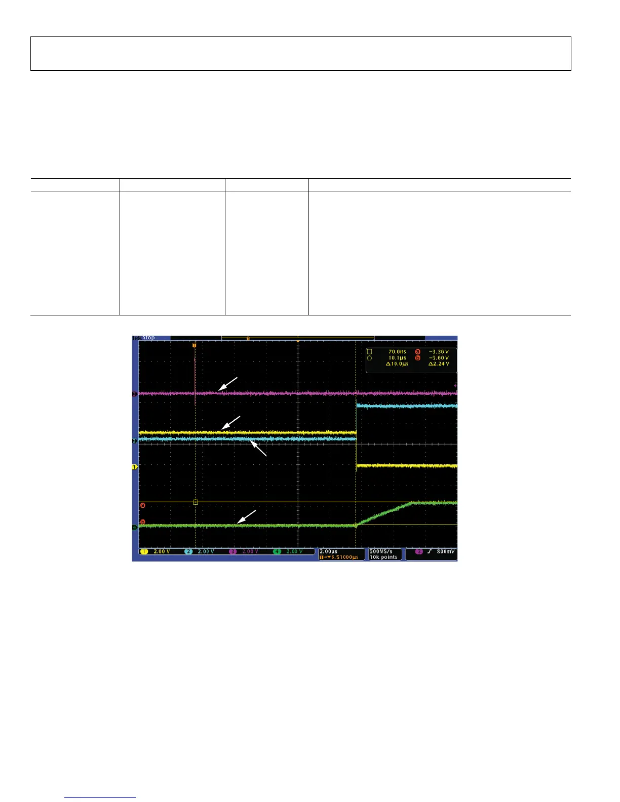
Figure 58 shows the timing of the GPOs and AuxDAC1 based
on the code written in Table 47 when the device transitions
from alert to receive. The pink trace shows when the ENABLE
pin is toggled. Note that after 10 µs, GPO0 (blue trace) and
GPO1 (yellow trace) change states and the AUXDAC (green
trace) starts ramping up to the desired voltage.
GPO Voltage Level, Drive Strength
The VDD_GPO pin (B8) which has a voltage range of 1.3 V to
3.3 V sets the output high logic level of the GPO. The off
resistance of the GPO pins is 15 Ω. The on resistance of the
GPO pins is 32 Ω.
Table 47. Example Code for Auto Toggle Timing of GPO and AuxDAC
Command Address(hex) Data(hex) Comment
SPI Write 27 02 Set all GPOs to 0 except GPO_1
SPI Write 26 0 Set GPO to auto mode
SPI Write 20 10 Set GPO_1 to 0 and GPO_0 to 1 in Rx
SPI Write 29 0A GPO_1 delay 10 µs in Rx
SPI Write 28 0A GPO_0 delay 10 µs in Rx
SPI Write 2C 0A GPO_0 delay 10 µs in Tx
SPI Write 2D 0A GPO_1 delay 10 µs in Tx
SPI Write 1A 1F Vref = 2.5 V, step factor = 1
SPI Write 18 7F AUXDAC Vout ~ 2.2 V
SPI Write 30 A AUXDAC1 delay =10 µs in Rx
Fig
ure 58. GPO/AuxDAC Toggle going from Alert to Rx
GPO0
GPO1
AUXDAC
ENABLE
11668-059

 Loading...


