UG-570 AD9361 Reference Manual
| Page 104 of 128
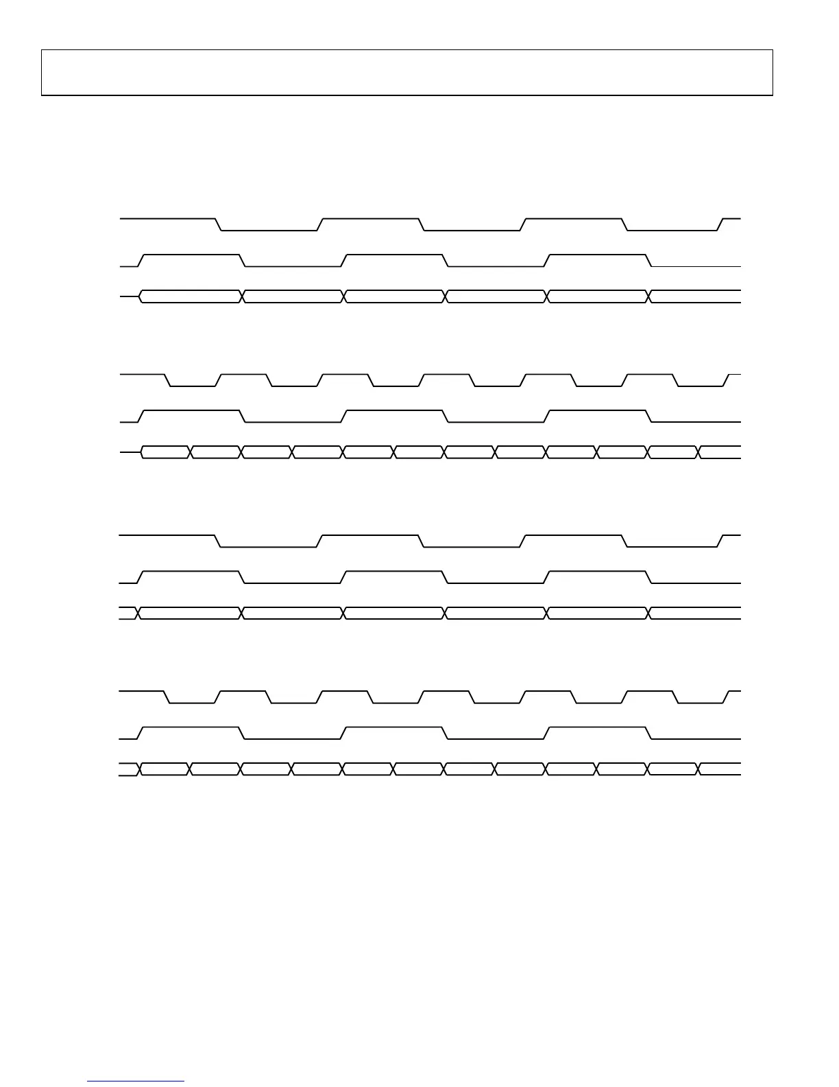
DUAL PORT FDD FUNCTIONAL TIMING (CMOS)
The timing diagrams in Figure 74 and Figure 75 illustrate the relationship among the bus signals in dual port full duplex mode. Note that
because 2R1T and 1R2T systems follow the 2R2T timing diagrams, they are omitted from Figure 74 and Figure 75.
Fig
ure 74. Receiver Data Path, Dual Port FDD (Full Port)
Fig
ure 75. Transmit Data Path, Dual Port FDD (Full Port)
DATA _CLK
RX _FRAME
P0 _D [11 :0 ]
DATA _CLK
RX _FRAME
P0 _D [11 :0 ]
1R1T, DDR, FDD, DUAL PORT, 0X010 = 0XC8, 0X011 = 0X00, 0X012 = 0X02
2R2T, DDR, FDD, DUAL PORT, 0X010 = 0XC8, 0X011 = 0X00, 0X012 = 0X02
R1_I[11:0] R1_Q[11:0] R1_I[11:0] R1_Q[11:0] R1_I[11:0] R1_Q[11:0]
R1_I[11:0] R1_Q[11:0] R1_I[11:0] R1_Q[11:0] R1_I[11:0] R1_Q[11:0] R1_I[11:0] R1_Q[11:0] R1_I[11:0] R1_Q[11:0] R1_I[11:0] R1_Q[11:0]
11668-075
FB _CLK
TX_FRAME
P0_D[11 :0]
FB
_CLK
TX_FRAME
P0_D [11 :0]
1R1T, DDR, FDD, DUAL PORT, 0X010 = 0XC8, 0X011 = 0X00, 0X012 = 0X02
2R2T, DDR, FDD, DUAL PORT, 0X010 = 0XC8, 0X011 = 0X00, 0X012 = 0X02
T1_I[11:0] T1_Q[11:0] T1_I[11:0] T1_Q[11:0] T1_I[11:0] T1_Q[11:0]
T1_I[11:0] T1_Q[11:0] T1_I[11:0] T1_Q[11:0] T1_I[11:0] T1_Q[11:0] T1_I[11:0] T1_Q[11:0] T1_I[11:0] T1_Q[11:0] T1_I[11:0] T1_Q[11:0]
11668-076
0
0

 Loading...


