UG-570 AD9361 Reference Manual
| Page 100 of 128
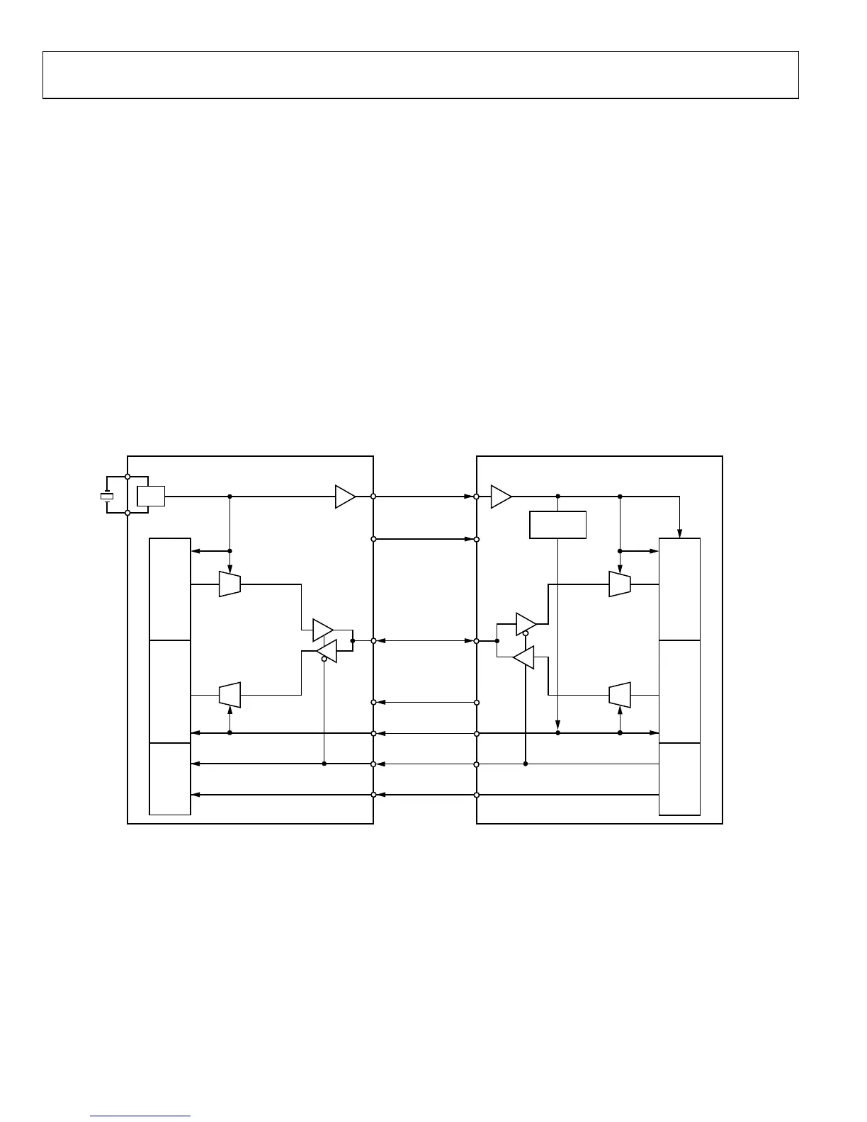
DUAL PORT HALF DUPLEX MODE (CMOS)
Dual port half duplex mode is used in applications requiring
TDD operation and data rates up to 122.88 MHz. In this mode,
both data ports are utilized, with P0 assigned to I data and P1
assigned to Q data. The ports operate bidirectionally in this
mode, and data direction is determined by which channel is
active: transmit or receive. Each bus can be operated as either
SDR or DDR in this configuration. This mode can be used with
all receiver-transmitter configurations. Figure 70 illustrates the
connections between the AD9361 and the BBP for this mode of
operation.
During an Rx burst, both ports are driven by the AD9361 such
that the setup and hold times between DATA_CLK and each
data sample arriving at the BBP enable the BBP to use
DATA_CLK to capture the data. A data transfer starts when the
ENABLE signal pulses (or goes high), and the end of the data
transfer is marked but another pulse on the ENABLE line (or
when it returns low).
The direction of data transfer is determined by the TXNRX
signal. When this signal is low and the AD9361 is in the FDD
state or the Rx state, the ENSM configures the bus in the receive
direction (data transferred from AD9361 to BBP). All other
states result in the bus being set to high impedance. When
TXNRX is driven high, the ENSM changes the bus to the
transmit direction (data transferred from BBP to AD9361).
During a transmit burst, both ports (P0_D[11:0] and
P1_D[11:0]) are driven by the BBP such that the setup and hold
times between FB_CLK and each D[11:0] allow the AD9361 to
use FB_CLK to capture the data.
The Rx_FRAME and Tx_FRAME signals indicate the
beginning of a set (frame) of data samples. The Rx_FRAME
signal can be set to occur once at the beginning of the burst
(one high transition only) or to have a rising edge at the
beginning of each frame and have a 50% duty cycle. Similarly,
Tx_FRAME accepts either format from the BBP.
Fig
ure 70. Dual Port TDD Mode
DATA_CLK
RX_FRAME
P0_D[11:0]
TX_FRAME
FB_CLK
TXNRX
ENABLE
RX
DATA
RX
DATA
TX
DATA
TX
DATA
CTRL CTRL
PLL
FEEDBACK
CLK GEN
AD9361
BBP
P1_D[11:0]
11668-072

 Loading...


