53
Operation
F-FEM-DDC — User’s Guide
4.8.5
Digital Outputs Transistor X53, X54
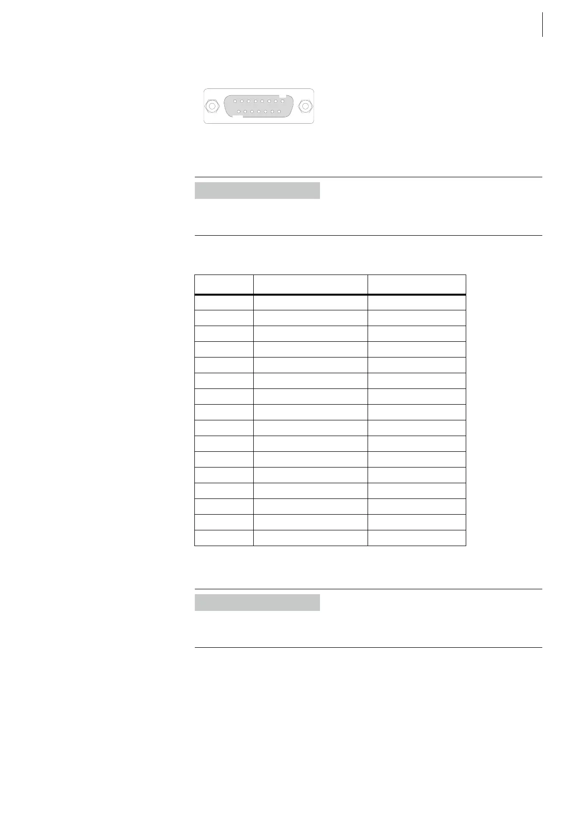
Pin assignment for digital outputs transistor X53, X54:
*) The total current for X53 and X54 all together is limited to 2.0 A.
Fig. 29
Information
The D-SUB jacks are equipped with a quick lock™ option for an easy click &
mount and a one hand remove mechanism.
Pin Signal at X53 Signal at X54
1 24 V out *) 24 V out *)
9 COMM_X53_V
CC
in COMM_X54_V
CC
in
2 24 V out *) 24 V out *)
10 Ch1 Ch1
3
11 Ch2 Ch2
4
12 Ch3 Ch3
5
13 Ch4 Ch4
6
14 Shield (opt.) Shield (opt.)
7 GND_24 out GND_24 out
15 COMM_X53_GNDin COMM_X54_GNDin
8 GND_24 out GND_24 out
Case Shield Shield
Tab. 20
Information
The maximum cross section of a wire soldered to a D-SUB connector pin is
limited to 0.5 mm² (equivalent to AWG 20 or more).
 Loading...