Safety
Information
Introduction
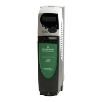
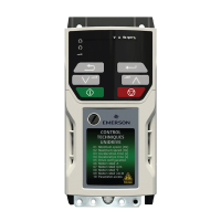
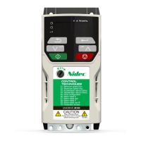
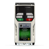
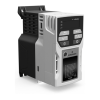
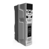
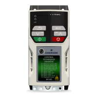
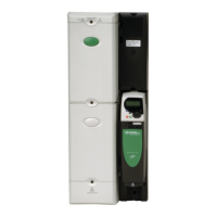
Product
Information
System
configuration
Mechanical
Installation
Electrical
Installation
Getting
Started
Basic
parameters
Running
the motor
Optimization
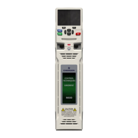
SMARTCARD
operation
Onboard
PLC
Advanced
parameters
Technical
Data
Diagnostics
UL Listing
Information
190 Unidrive SPM User Guide
www.controltechniques.com Issue Number: 3
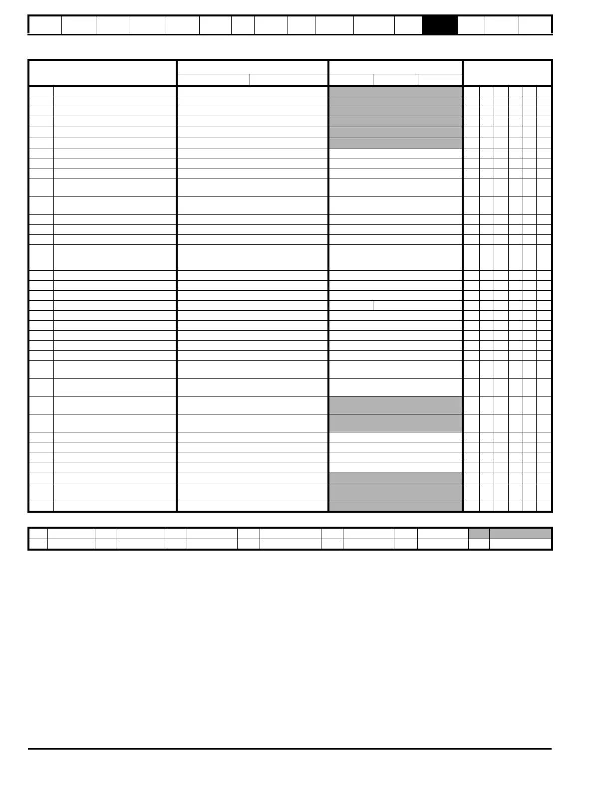
Parameter
Range(
Ú) Default(Ö)
Type
OL CL OL VT SV
7.01 T5/6 analog input 1 level ±100.00 %
RO Bi NC PT
7.02 T7 analog input 2 level ±100.0 %
RO Bi NC PT
7.03 T8 analog input 3 level ±100.0 %
RO Bi NC PT
7.04 Power circuit temperature 1
-128 to 127
°C
RO Bi NC PT
7.05 Power circuit temperature 2
-128 to 127
°C
RO Bi NC PT
7.06 Control board temperature
-128 to 127
°C
RO Bi NC PT
7.07 T5/6 analog input 1 offset trim {0.13} ±10.000 % 0.000 RW Bi US
7.08 T5/6 analog input 1 scaling 0 to 4.000 1.000 RW Uni US
7.09 T5/6 analog input 1 invert OFF (0) or On (1) OFF (0) RW Bit US
7.10
T5/6 analog input 1
destination
Pr 0.00 to 21.51 Pr 1.36 RW Uni DE PT US
7.11 T7 analog input 2 mode {0.19}
0-20 (0), 20-0 (1), 4-20.tr (2), 20-4.tr (3),
4-20 (4), 20-4 (5), VOLt (6)
VOLt (6) RW Txt US
7.12 T7 analog input 2 scaling 0 to 4.000 1.000 RW Uni US
7.13 T7 analog input 2 invert OFF (0) or On (1) OFF (0) RW Bit US
7.14 T7 analog input 2 destination {0.20}Pr 0.00 to 21.51 Pr 1.37 RW Uni DE PT US
7.15 T8 analog input 3 mode {0.21}
0-20 (0), 20-0 (1), 4-20.tr (2), 20-4.tr (3),
4-20 (4), 20-4 (5), VOLt (6), th.SC (7),
th (8), th.diSP (9)
th (8) RW Txt US
7.16 T8 analog input 3 scaling 0 to 4.000 1.000 RW Uni US
7.17 T8 analog input 3 invert OFF (0) or On (1) OFF (0) RW Bit US
7.18 T8 analog input 3 destination Pr 0.00 to 21.51 Pr 0.00 RW Uni DE PT US
7.19 T9 analog output 1 source Pr 0.00 to 21.51 Pr 5.01 Pr 3.02 RW Uni PT US
7.20 T9 analog output 1 scaling 0.000 to 4.000 1.000 RW Uni US
7.21 T9 analog output 1 mode VOLt (0), 0-20 (1), 4-20 (2), H.SPd (3) VOLt (0) RW Txt US
7.22 T10 analog output 2 source Pr 0.00 to 21.51 Pr 4.02 RW Uni PT US
7.23 T10 analog output 2 scaling 0.000 to 4.000 1.000 RW Uni US
7.24 T10 analog output 2 mode VOLt (0), 0-20 (1), 4-20 (2), H.SPd (3) VOLt (0) RW Txt US
7.25
Calibrate T5/6 analog input 1
full scale
OFF (0) or On (1) OFF (0) RW Bit NC
7.26
T5/6 analog input 1 sample
time
0 to 8.0 ms 4.0 RW Uni US
7.28
T7 analog input 2 current loop
loss
OFF (0) or On (1)
RO Bit NC PT
7.29
T8 analog input 3 current loop
loss
OFF (0) or On (1)
RO Bit NC PT
7.30 T5/6 analog input 1 offset ±100.00 % 0.00 RW Bi US
7.31 T7 analog input 2 offset ±100.0 % 0.0 RW Bi US
7.32 T8 analog input 3 offset ±100.0 % 0.0 RW Bi US
7.33 T9 analog output 1 control Fr (0), Ld (1), AdV (2) AdV (2) RW Txt US
7.34 IGBT junction temperature
±200
°C
RO Bi NC PT
7.35
Drive thermal protection
accumulator
0 to 100.0 %
RO Uni NC PT
7.36 Power circuit temperature 3
-128 to 127
°C
RO Bi NC PT
RW Read / Write RO Read only Uni Unipolar Bi Bi-polar Bit Bit parameter Txt Text string
FI Filtered DE Destination NC Not copied RA Rating dependent PT Protected US User save PS Power down save
 Loading...