MC68332 ELECTRICAL CHARACTERISTICS
USER’S MANUAL A-21
NOTE: AS and DS timing shown for reference only.
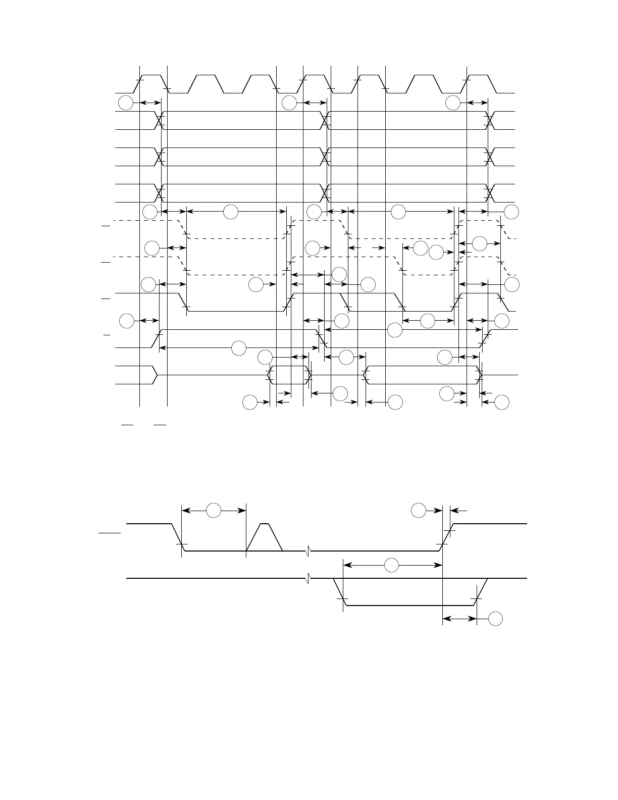
Figure A-11 Chip Select Timing Diagram
Figure A-12 Reset and Mode Select Timing Diagram
68300 CHIP SEL TIM
S0 S1 S2 S3 S4 S5 S0 S1 S2 S3 S4 S5
CLKOUT
A0–A23
FC0–FC2
SIZ0, SIZ1
AS
DS
CS
R/W
D0–D15
66
8
11
12
13
99
14
11
9
14
15
25
20
18
17
12 21
17
18
21
23
29A
27
53
54
46
55
29
14A
46
68300 RST/MODE SEL TIM
RESET
D0–D15
75
77 78
76
Fr
ees
cale S
em
iconduct
or
, I
Freescale Semiconductor, Inc.
For More Information On This Product,
Go to: www.freescale.com
nc...