Clocking
R
138 Intel
®
815 Chipset Platform Design Guide
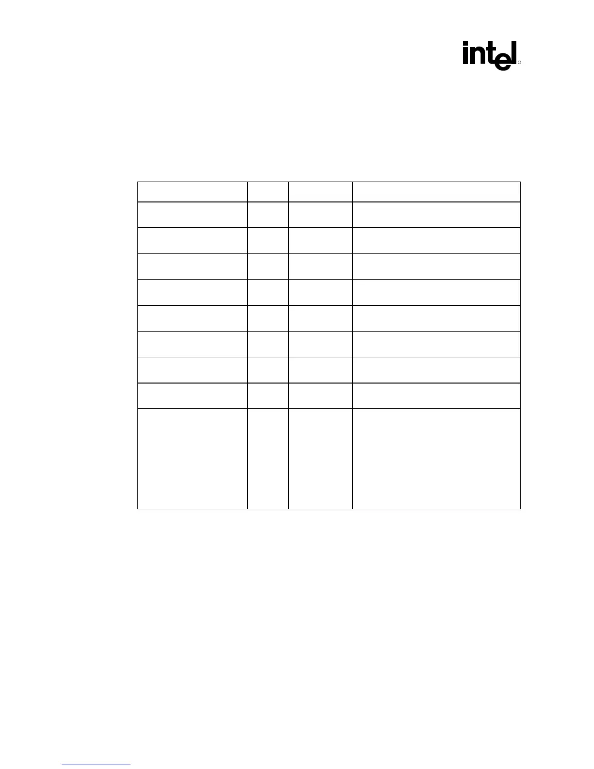
11.6 Clock Skew Assumptions
The clock skew assumptions in the following table are used in the system clock simulations.
Table 31. Simulated Clock Skew Assumptions
Skew Relationships Target Tolerance (±) Notes
HCLK @ GMCH to HCLK
@ processor
0 ns 200 ps • Assumes ganged clock outputs will allow
maximum of 50 ps skew
HCLK @ GMCH to SCLK
@ GMCH
0 ns 600 ps • 500 ps pin-to-pin skew
• 100 ps board/package skew
SCLK @ GMCH to SCLK
@ SDRAM
0 ns 630 ps • 250 ps pin-to-pin skew
• 380 ps board + DIMM variation
HLCLK @ GMCH to SCLK
@ GMCH
0 ns 900 ps • 500 ps pin-to-pin skew
• 400 ps board/package skew
HLCLK @ GMCH to HCLK
@ GMCH
0 ns 700 ps • 500 ps pin-to-pin skew
• 200 ps board/package skew
HLCLK @ GMCH to HLCLK
@ ICH
0 ns 375 ps • 175 ps pin-to-pin skew
• 200 ps board/package skew
HLCLK @ ICH to PCICLK
@ ICH
0 ns 900 ps • 500 ps pin-to-pin skew
• 400 ps board/package skew
PCICLK @ ICH to PCICLK
@ other PCI devices
0 ns 2.0 ns window • 500 ps pin-to-pin skew
• 1.5 ns board/add-in skew
HLCLK @ GMCH to
AGPCLK @ connector
• Total electrical length of AGP connector +
add-in card is 750 ps (according to
AGP2.0 specification and AGP design
guide 1.0).
• Motherboard clock routing must account
for this additional electrical length.
Therefore, AGPCLK routed to the
connector must be shorter than HLCLK to
the GMCH, to account for this additional
750 ps.