Component Quadrant Layouts
R
28 Intel
®
815 Chipset Platform Design Guide
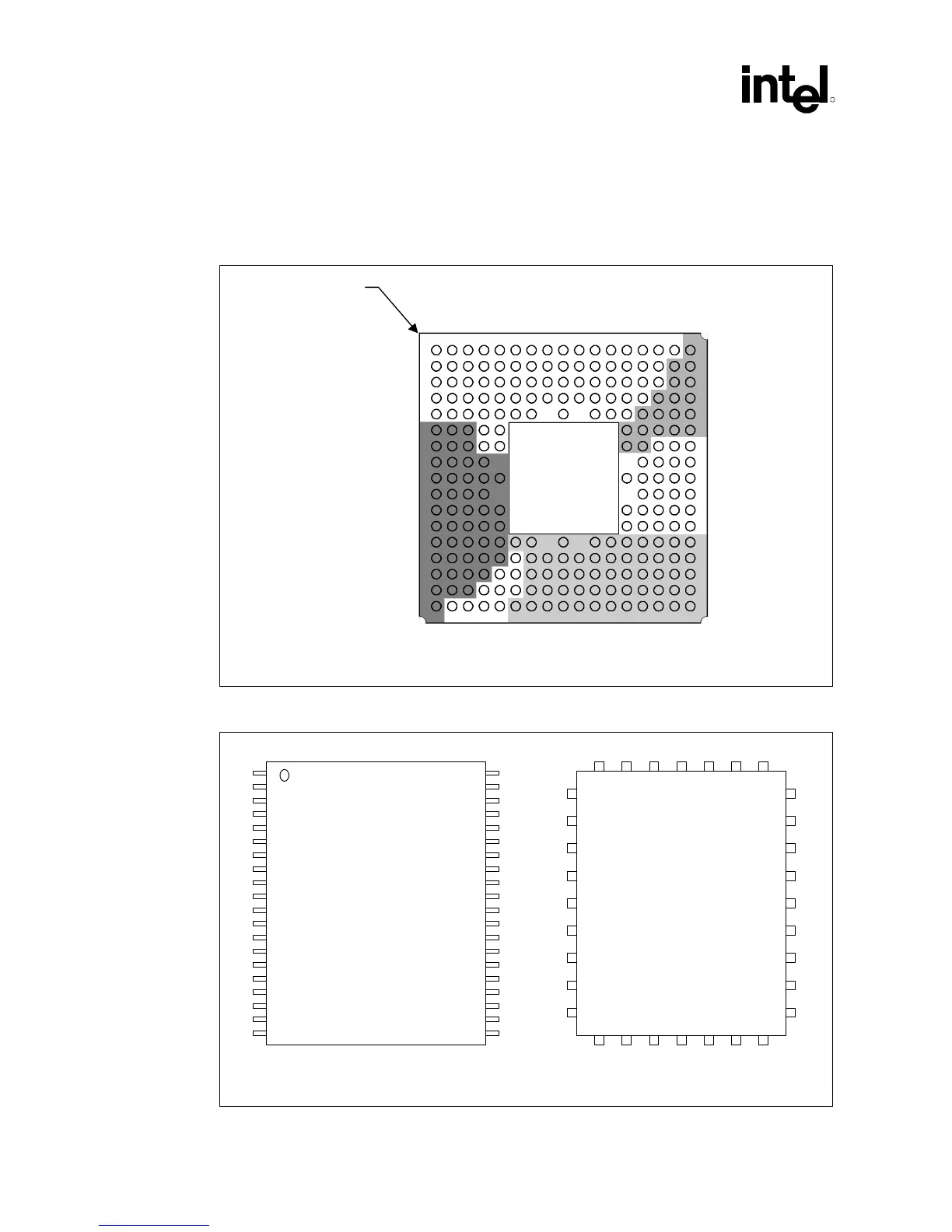
Figure 5 illustrates the relative signal quadrant locations on the ICH ballout. It does not represent
the actual ballout. Refer to the Intel
®
82801AA (ICH) and 82801AB (ICH0) I/O Controller Hub
Datasheet for the actual ballout.
Figure 5. ICH 241-Ball µ
µµ
µBGA* CSP Quadrant Layout (Top View)
quad_ICH
PCI
Pin 1 corner
Processor
Hub interface
ICH
IDE
LPC
AC'97,
SMBus
Figure 6. Firmware Hub (FWH) Packages
pkg_FWH
5
6
7
8
9
10
11
12
13
29
28
27
26
25
24
23
22
21
1234323130
14 15 16 17 18 19 20
FWH interface
(32-lead PLCC,
0.450" x 0.550")
Top view
1
2
3
4
5
6
7
8
9
10
11
12
13
14
15
16
17
18
19
20
40
39
38
37
36
35
34
33
32
31
30
29
28
27
26
25
24
23
22
21
FWH interface
(40-lead TSOP)