System Design Checklist
R
Intel
®
815 Chipset Platform Design Guide 167
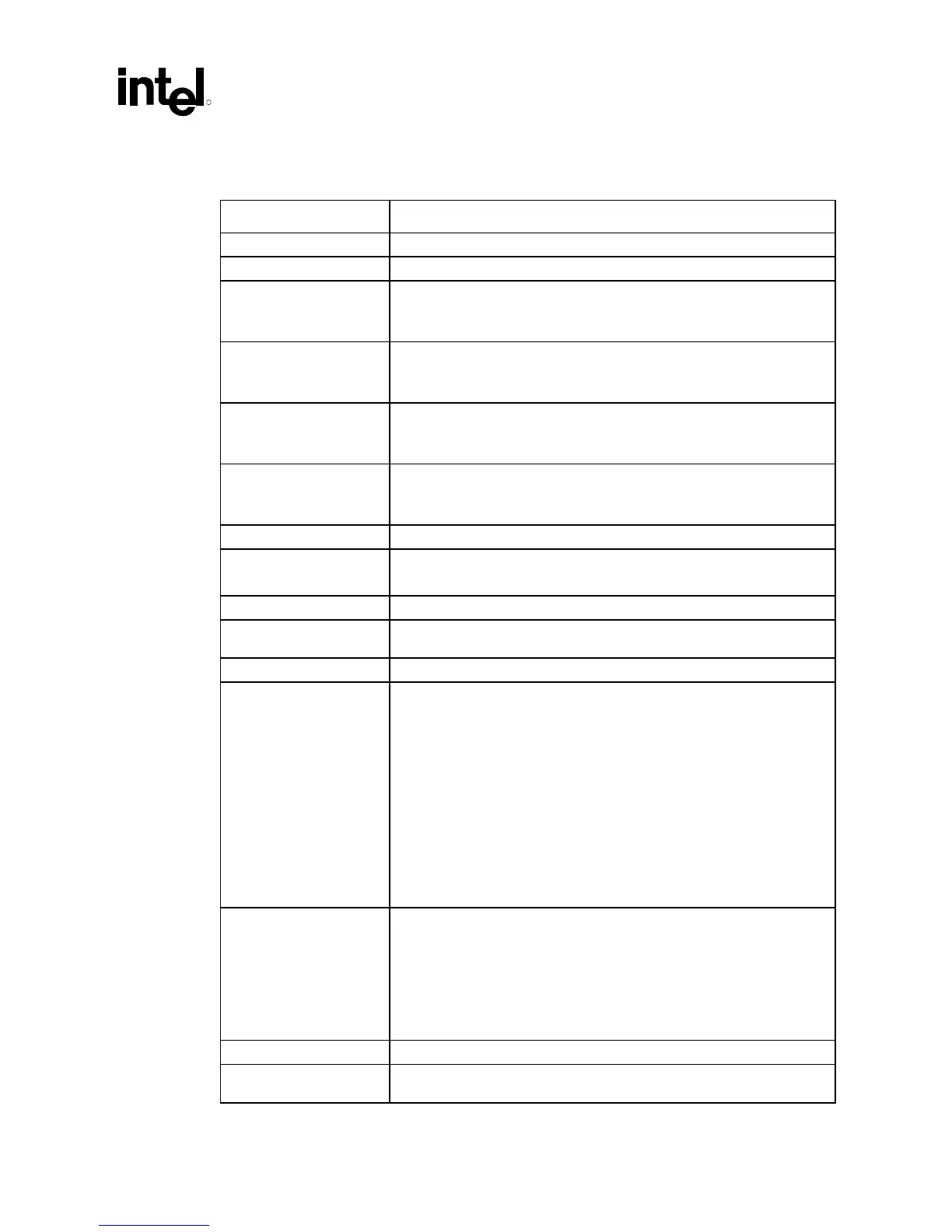
13.8 Clock Synthesizer Checklist
Checklist Items Recommendations
REFCLK • Connects to R-RefCLK, USB_CLK, SIO_CLK14, and ICHCLK14.
GMCH_3V66/3V66_1 • Passes through 33 Ω resistor
ICH_3V66/3V66_0,
DOTCLK
• Passes through 33 Ω resistor
• When signal is input for ICH it is pulled down through a 18 pF capacitor to
GND
DCLK/DCLK_WR • Passes through 33 Ω resistor
• When signal is input for GMCH it is pulled down through a 22 pF capacitor
to GND
CPUHCLK/CPU_0_1 • Passes through 33 Ω resistor
• When signal is input for 370PGA, Decouple through a 18 pF capacitor to
GND
R_REFCLK • REFCLK passed through 10 kΩ resistor
• When signal is input for 370PGA, pull-up through 1 kΩ resistor to VCC3_3
and pass through 10 kΩ resistor
USB_CLK, ICH_CLK14 • REFCLK passed through 10 Ω resistor
XTAL_IN, XTAL_OUT • Passes through 14.318 MHz Osc
• Pulled down through 18 pF capacitor to GND
SEL1_PU • Pulled up via MEMV3 circuitry through 8.2 kΩ resistor.
FREQSEL • Connected to clock frequency selection circuitry through 10 kΩ resistor.
(see CRB schematic, page 4)
L_VCC2_5 • Connects to VDD2_5[0..1] through ferrite bead to VCC2_5.
GMCHHCLK/CPU_1,
ITPCLK/CPU_2,
PCI_0/PCLK_OICH,
PCI_1/PCLK_1,
PCI_2/PCLK_2,
PCI_3/PCLK_3,
PCI_4/PCLK_4,
PCI_5/PCLK_5,
PCI_6/PCLK_6,
APICCLK_CPU/APIC_0,
APICCLK)ICH/APIC_1,
USBCLK/USB_0,
GMCH_3V66/3V66_1,
AGPCLK_CONN
• Passes through 33 Ω resistor
MEMCLK0/DRAM_0,
MEMCLK1/DRAM_1,
MEMCLK2/DRAM_2,
MEMCLK3/DRAM_3,
MEMCLK4/DRAM_4,
MEMCLK5/DRAM_5,
MEMCLK6/DRAM_6,
MEMCLK7/DRAM_7,
• Pass through 10 Ω resistor
SCLK • Pass through 22 Ω resistor.
VCC3.3 • Connected to VTTPWRGD gating circuit as per Section 4.3.1 for systems
supporting the
universal PGA370 design.