System Design Checklist
R
160 Intel
®
815 Chipset Platform Design Guide
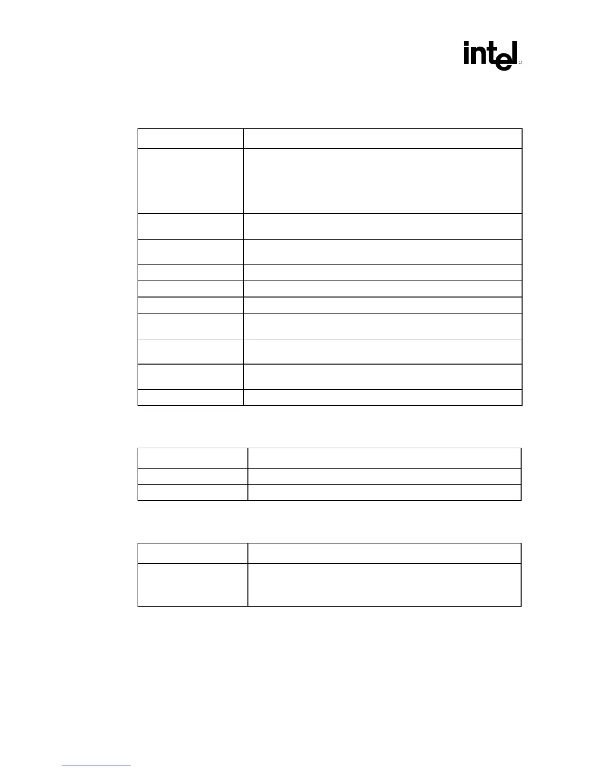
13.3.3 System Memory Interface Checklist
Checklist Items Recommendations
SM_CSA#[0:3,
SM_CSB#[3:0,
SMAA[11:8,3:0],
SM_MD[0:63],
SM_CKE[0:3],
S_DQM[0:7]
• Connect from GMCH to DIMM0, DIMM1
SM_MAA[7:4],
SM_MAB[7:4]#
• Connect from GMCH to DIMM0, DIMM1 through 10 ohm resistors
SMAA[12] • Connect GMCH through 10 kΩ resistor to transistor junction as per
Chapter 4
for systems supporting the universal PGA370 design.
SM_CAS# • Connected to R_REFCLK through 10 kΩ resistor.
SM_RAS# • Jumpered to GND through 10 kΩ resistor
SM_WE# • Connected to R_BSEL0# through 10 kΩ resistor.
CKE[5..0] (For 3 DIMM
implementation)
• When implementing a 3 DIMM configuration, all six CKE signals on the
GMCH are used. (0,1 for DIMM0; 2, 3 for DIMM1; 4,5 for DIMM2)
REGE • Connect to GND (since the Intel
®
815 chipset platform does not support
registered DIMMS).
WP(Pin 81 on the DIMMS) • Add a 4.7 kΩ pull-up resistor to 3.3V. This recommendation write-protects
the DIMM’s EEPROM.
SRCOMP • Needs a 40 Ω resistor pulled up to 3.3V standby.
13.3.4 Hub Interface Checklist
Checklist Items Recommendations
HUBREF • Connect to HUBREF generation circuitry.
HL_COMP • Pull-up to VCC1.85 through 40 Ω (both GMCH and ICH side).
13.3.5 Digital Video Output Port Checklist
Checklist Items Recommendations
DVI Input Reference Circuit • See reference schematics in the documentation of the third party vendor
of the device of choice in your design. The Third-Party Vendor
information is a part of this Design Guide and its associated Design
Guide Updates.