System Bus Design Guidelines
R
Intel
®
815 Chipset Platform Design Guide 61
5.9.3 Recommendation for Intel Platforms
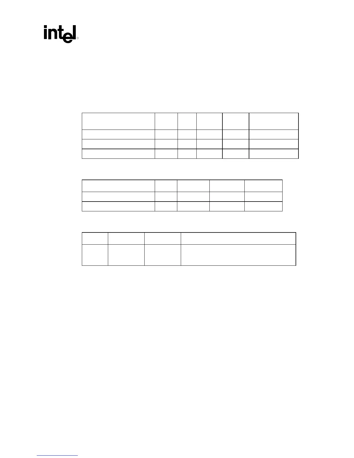
The following tables contain examples of components that meet Intel’s recommendations, when
configured in the topology of Figure 27.
Table 15. Component Recommendations – Inductor
Part Number Value Tol. SRF Rated
Current
DCR (Typical)
TDK MLF2012A4R7KT 4.7 µH 10% 35 MHz 30 mA 0.56 Ω (1 Ω max.)
Murata LQG21N4R7K00T1 4.7 µH 10% 47 MHz 30 mA 0.7 Ω (± 50%)
Murata LQG21C4R7N00 4.7 µH 30% 35 MHz 30 mA 0.3 Ω max.
Table 16. Component Recommendations – Capacitor
Part Number Value Tolerance ESL ESR
Kemet T495D336M016AS 33 µF 20% 2.5 nH 0.225 Ω
AVX TPSD336M020S0200 33 µF 20% 2.5 nH 0.2 Ω
Table 17. Component Recommendation – Resistor
Value Tolerance Power Note
1 Ω 10% 1/16 W Resistor may be implemented with trace resistance,
in which case a discrete R is not needed. See
Figure 28.
To satisfy damping requirements, total series resistance in the filter (from VCC
CORE
to the top plate
of the capacitor) must be at least 0.35 Ω. This resistor can be in the form of a discrete component
or routing or both. For example, if the chosen inductor has a minimum DCR of 0.25 Ω, then a
routing resistance of at least 0.10 Ω is required. Be careful not to exceed the maximum resistance
rule (2 Ω). For example, if using discrete R1 (1 Ω ± 1%), the maximum DCR of the L (trace plus
inductor) should be less than 2.0 - 1.1 = 0.9 Ω; this precludes the use of some inductors and sets a
maximum trace length.
Other routing requirements:
• The capacitor (C) should be close to the PLL1 and PLL2 pins, < 0.1 Ω per route. These routes
do not count towards the minimum damping R requirement.
• The PLL2 route should be parallel and next to the PLL1 route (i.e., minimize loop area).
• The inductor (L) should be close to C. Any routing resistance should be inserted between
VCC
CORE
and L.
• Any discrete resistor (R) should be inserted between VCC
CORE
and L.