System Bus Design Guidelines
R
56 Intel
®
815 Chipset Platform Design Guide
5.5 BSEL[1:0] Implementation Differences
A future 0.13 micron socket 370 processor will select the 133 MHz system bus frequency setting
from the clock synthesizer. A Pentium III processor (CPUID=068xh) utilizes the BSEL1 pin to
select either the 100 MHz or 133 MHz system bus frequency setting from the clock synthesizer.
An Celeron processor (CPUID=068xh) will use both BSEL pins to select 66 MHz system bus
frequency from the clock synthesizer. Processors in an FC-PGA or an
FC-PGA2 are 3.3V tolerant for these signals, as are the clock and chipset.
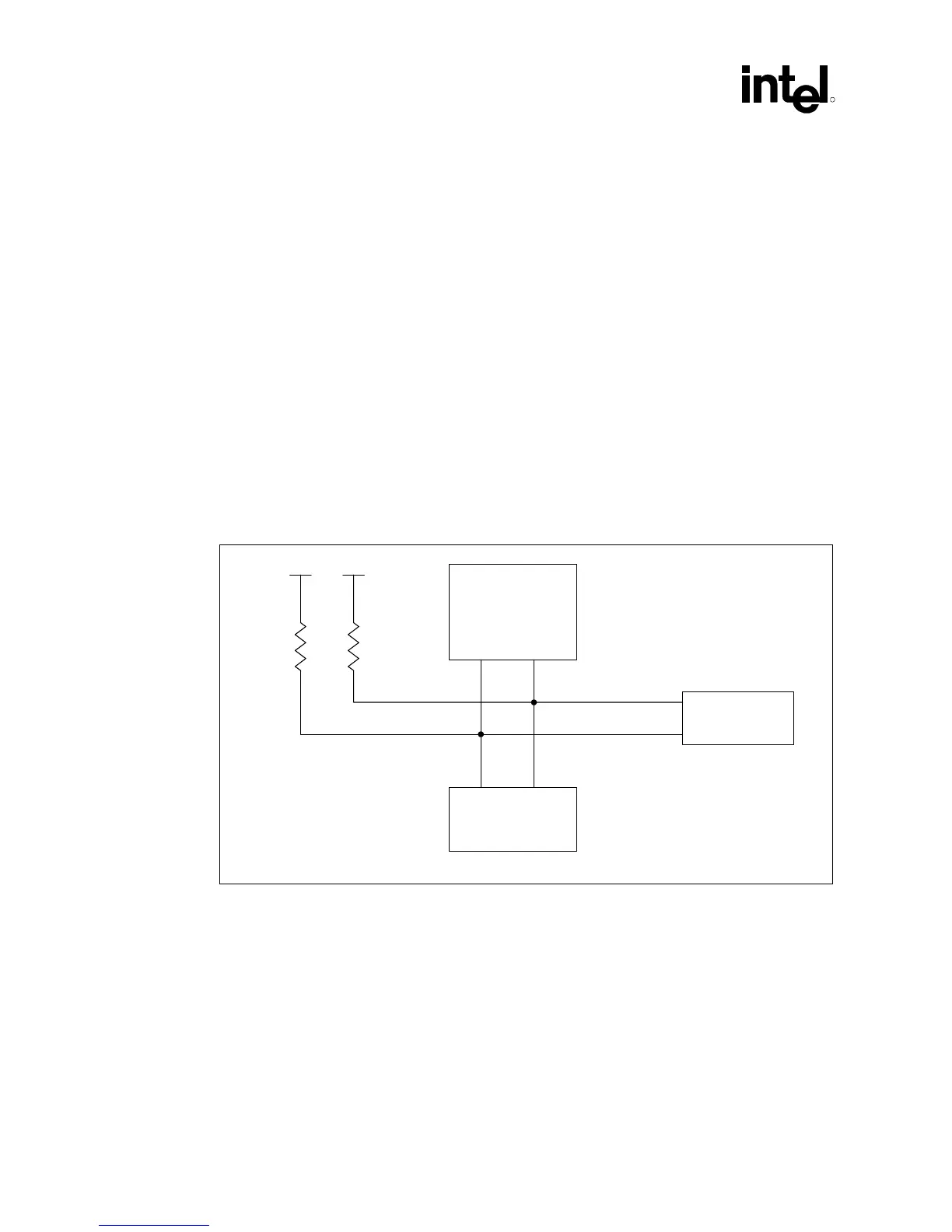
Intel CK-815 has been designed to support selections of 66 MHz, 100 MHz, and 133 MHz. The
REF input pin has been redefined to be a frequency selection strap (BSEL1) during power-on and
then becomes a 14 MHz reference clock output. The following figure details the new BSEL[1:0]
circuit design for universal PGA370 designs. Note that BSEL[1:0] now are pulled up using 1 kΩ
resistors. Also refer to Figure 24 for more details.
Note: In a design supporting future 0.13 micron socket 370 processors, the BSEL[1:0] lines are not valid
until VTTPWRGD is asserted. Refer to Section 4.2.10 for details.
Figure 23. BSEL[1:0] Circuit Implementation for PGA370 Designs
Processor
BSEL0 BSEL1
Chipset
Clock Driver
1 kΩ1 kΩ
3.3V
sys_ bus_BSEL_PGA370
3.3V