System Design Checklist
R
168 Intel
®
815 Chipset Platform Design Guide
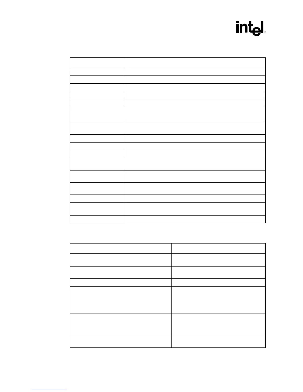
13.9 LAN Checklist
Checklist Items Recommendations
TDP, TDN, RDP, RDN • Pull-down through 50 Ω resistor to GND
LANAPWR • Passes through 3 kΩ resistor
LANCLKRUN • Pull-down through 62 kΩ resistor
LAN_ISOLATE# • Connect to SUS_STAT# and PWROK
LAN_TEST • Pull-down through a 4.7 kΩ resistor to GND
LAN_XTAL1, LAN_XTAL2 • Signal from 25 MHz oscillator
• Decouple through a 22 pF capacitor to GND
FLD5_PD, FLD6_PD,
RBIAS10, RBIAS100
• Pull-down through a 619 Ω resistor to GND
ACTLED/LI_CR • Passes through 330 Ω resistor
LILED • Connect to jumper, pull-up through 330 Ω resistor to VCC3SBY
ACT_CR • Pull-up through 330 Ω resistor to VCC3SBY
RD_PD • Pull-down RDP through 50 Ω resistor and to RDN through 50 Ω resistor to
GND
TD_PD • Pull-down TDP through 50 Ω resistor and to TDN through 50 Ω resistor to
GND
SPEEDLED • Connect LED anode to VCC3SBY through 330 Ω resistor and cathode to
Intel
®
82559. Jumper to VCC3SBY through 330 Ω resistor
CHASSIS_GND • Use plane for this signal.
JP7_PU, JP18_PU,
JP23_PU
• Pull-up through 330 Ω resistor to VCC3SBY
R_LANIDS • Pass through 100 Ω resistor to AD20 from Intel 82559 pin IDSEL.
13.10 Power Delivery Checklist
Checklist Items Recommendations
All voltage regulator components meet maximum
current requirements
• Consider all loads on a regulator, including
other regulators.
All regulator components meet thermal requirements • Ensure the voltage regulator components and
dissipate the required amount of heat.
VCC1_8 • VCC1_8 power sources must supply 1.85V
If devices are powered directly from a dual rail
(i.e., not behind a power regulator), then the RDSon
of the FETs used to create the dual rail must be
analyzed to ensure there is not too much voltage drop
across the FET.
• “Dual” voltage rails may not be at the expected
voltage.
Dropout Voltage • The minimum dropout for all voltage regulators
must be considered. Take into account that the
voltage on a dual rail may not be the expected
voltage.
Voltage tolerance requirements are met • See individual component specifications for
each voltage tolerance.