AGP/Display Cache Design Guidelines
R
94 Intel
®
815 Chipset Platform Design Guide
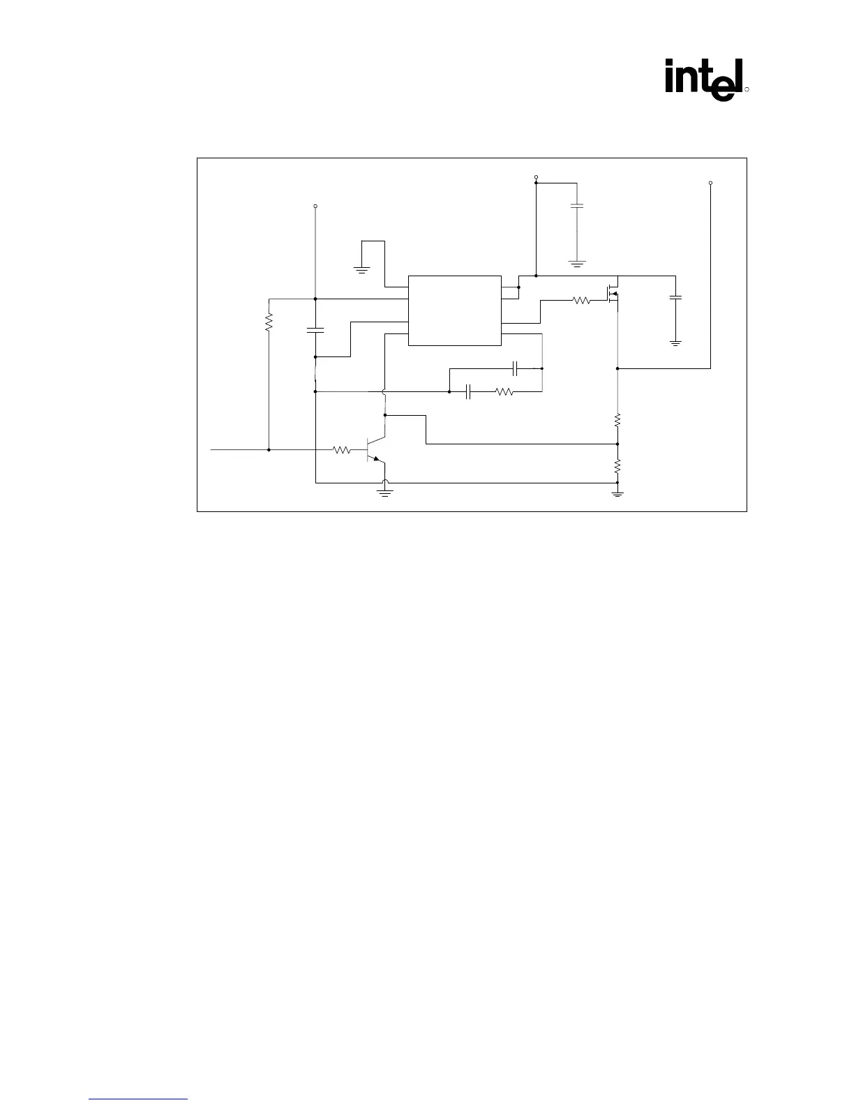
Figure 46. AGP VDDQ Generation Example Circuit
SHDN IPOS
VIN INEG
GND GATE
FB COMP
C1
2.2 k
Ω
10 pF
C2
5
R3
R4
C3
+12V
+3.3V
VDDQ
R1
1 µF
TYPEDET#
U1
LT1575
1
2
3
4
8
7
6
5
C5
R5
C4
R2
301 - 1%
1.21 k
Ω
- 1%
47 µF
220 µF
AGP_VDDQ_gen_ex_circ
.001 µF
7.5 k
Ω
- 1%
The previous figure demonstrates one way to design the VDDQ voltage regulator. This regulator
is a linear regulator with an external, low-Rds
on
FET. The source of the FET is connected to 3.3V.
This regulator converts 3.3V to 1.5V or passes 3.3V, depending on the state of TYPEDET#. If a
linear regulator is used, it must draw power from 3.3V (not 5V) to control thermals
(i.e., 5V regulated down to 1.5V with a linear regulator will dissipate approximately 7 W at 2 A).
Because it must draw power from 3.3V and, in some situations, must simply pass that 3.3V to
VDDQ (when a 3.3V add-in card is placed in the system), the regulator MUST use a low-Rds
on
FET.
AGP 1.0 ECR #44 modified VDDQ 3.3
min
to 3.1V. When an ATX power supply is used, the
3.3 V
min
is 3.168V. Therefore, 68 mV of drop is allowed across the FET at 2 A. This corresponds
to a FET with an Rds
on
of 34 mΩ.
How does the regulator switch? The feedback resistor divider is set to 1.5V. When a 1.5V card
is placed in the system, the transistor is Off and the regulator regulates to 1.5V. When a 3.3V card
is placed in the system, the transistor is On, and the feedback will be pulled to ground. When this
happens, the regulator will drive the gate of the FET to nearly 12V. This will turn the FET on and
pass 3.3V – (2 A * Rds
on
) to VDDQ.