Hardware Operations
2015-MNU-000009
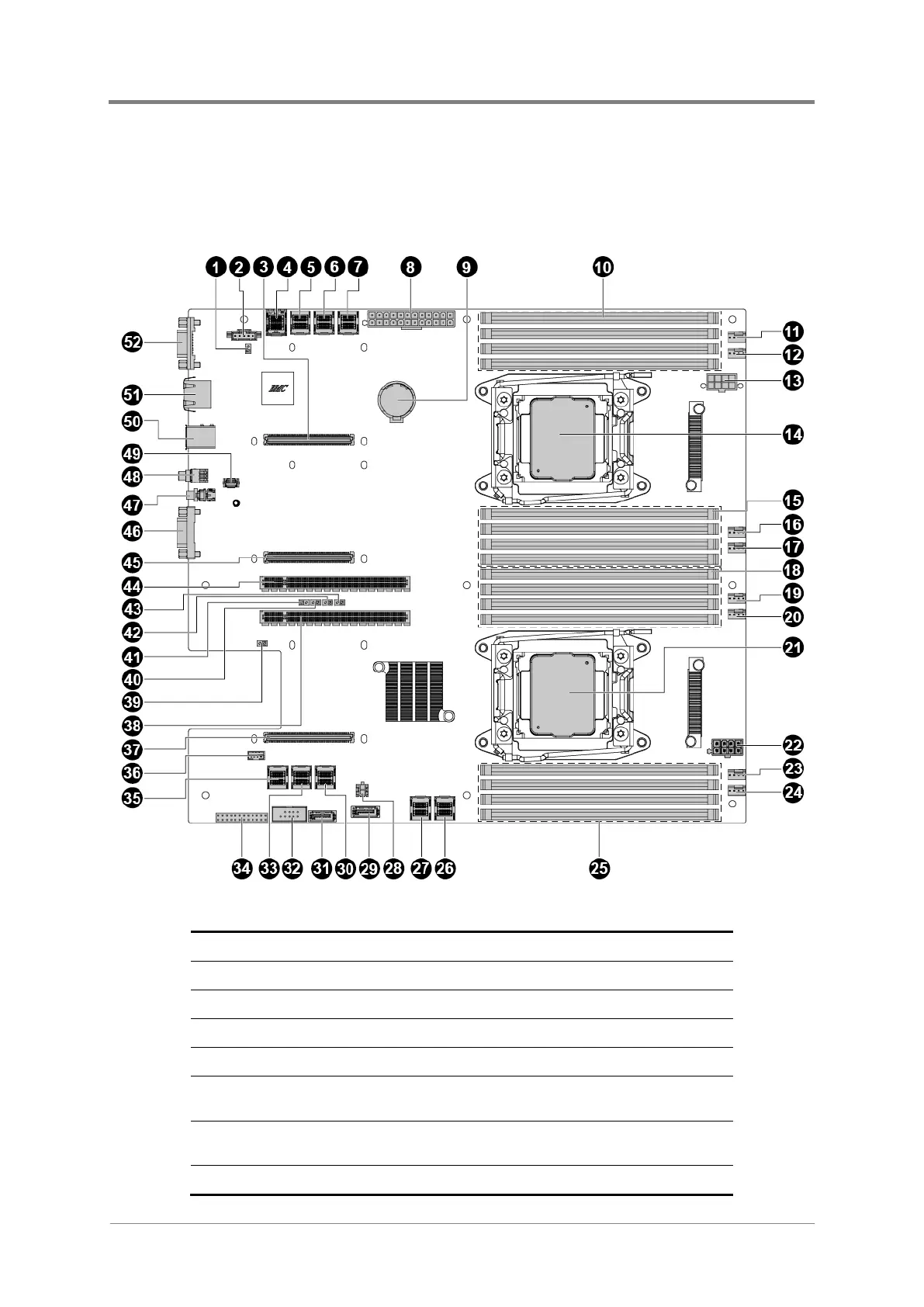
1.4 Motherboard Layout
The layout of the motherboard is shown below. Each connector and major component is
identified by number.
Figure 1-2 Connector and Component Location of Motherboard
3 CPU1 NIC OCP Slot (J75)
CPU1 PE2A HD_MiniSAS Connector (J79)
5 CPU1 PE2B HD_MiniSAS Connector (J78)
6
CPU1 PE2C HD_MiniSAS Connector (J76) (on SKU 301
motherboard; not featured on SKU 302)
7
CPU1 PE2D HD_MiniSAS Connector (J77) (on SKU 301
motherboard; not featured on SKU 302)
 Loading...