44
GENERAL ELECTRICAL DATA
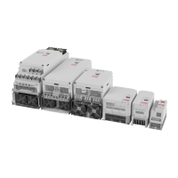
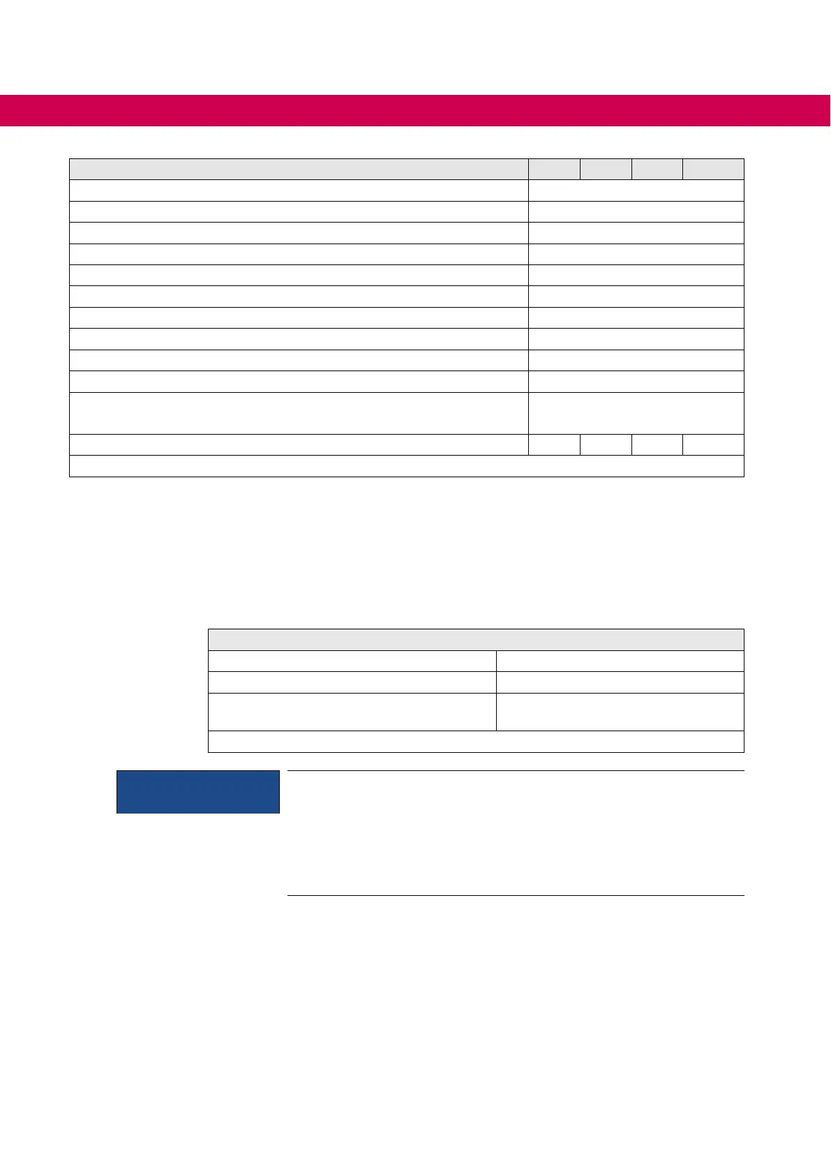
Device size 21 22 23 24
Rated DC link voltage @ U
N = 400V UN_dc / V 565
Rated DC link voltage @ U
N_UL = 480V U
N_dc_UL
/ V 680
DC link voltage working voltage range U
IN_dc / V 390...780
DCswitch-olevel"ERRORunderpotential“ U
UP / V 240
DCswitch-olevel"ERRORoverpotential“ U
OP / V 840
DCswitch-olevelbrakingtransistor
1)
UB / V 780
Max. braking current I
B_max / A 168
Min. braking resistor value R
B_min/Ω 5
Braking transistor
2)
Max.cycletime:120s;ED:50%
Protection function for braking transistor Short-circuit monitoring
Protection function braking transistor
(Error GTR7 always on)
3)
Feedback signal evaluation and
current shutdown
DC link capacity C / µF 3300 3900 5200 6200
Table 24: DC link / braking transistor function of the 400 V devices
1)
The DC switching level for the braking transistor is adjustable. The default value is the value specied in the
table.
2)
The ON time is additionally limited by the used braking resistor
3)
The feedback signal evaluation monitors the functionality of the braking transistor. The current is switched
o via the internal mains input bridge of the AC supply.
3.3.3 Sub-mounted braking resistors
Technical data of the sub-mounted braking resistors
Braking resistor value R/Ω 8
Rated power P
D / W 730
Cyclic duration factor referring to
120s @ U
_dc = 780V
ED / s 0.9
Table 25: Sub-mounted braking resistors
NOTICE
Observe the power dissipation of the sub-mounted braking resis-
tors
In braking mode with sub-mounted braking resistors, the power to be
dissipated of the heat sink will be increased.
► Consider the power dissipation of the braking resistors when de-
signing the cooling system.
 Loading...