List of Figures
ix
List of Figures
Figure 1: Voltage and Fuse Data for the Low Power Unit...................................................... 25
Figure 2: Voltage and Fuse Data for the High Power Unit ..................................................... 26
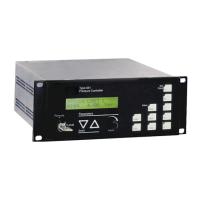
Figure 3: Front Panel of the 651 Instrument........................................................................... 27
Figure 4: Rear Panel of the 651 Instrument............................................................................ 31
Figure 5: Serial Number Label .............................................................................................. 38
Figure 6: I/O Board Digital Input Circuitry............................................................................ 90
Figure 7: I/O Board Digital Output Circuitry......................................................................... 91
Figure 8: Location of the Battery-backed RAM Module........................................................ 98
Figure 9: Initial Display Screen............................................................................................. 103
Figure 10: Default Pressure and Position Screen.................................................................... 103
Figure 11: Battery Voltage Low Message.............................................................................. 104
Figure 12: Battery Voltage High Message ............................................................................. 104
Figure 13: Fuse Holder.......................................................................................................... 112
Figure 14: Front Panel of the 651 Displayless Unit................................................................ 119
Figure 15: Dipswitch Bank Location (Top View) .................................................................. 121
Figure 16: Example of Dipswitch Bank................................................................................. 121