Do you have a question about the Philips BJ3.0E and is the answer not in the manual?
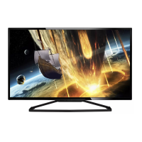
| Aspect Ratio | 16:9 |
|---|---|
| Brightness | 250 cd/m² |
| Resolution | 1920 x 1080 pixels |
| Contrast Ratio | 1000:1 |
| Connectivity | VGA, HDMI |
| Input Ports | VGA, HDMI |
Details on vision, sound, and miscellaneous specifications for the television chassis.
Details on rear and side connections, including HDMI, USB, and SCART ports.
Overview of the chassis with locations of main Printed Wiring Boards (PWBs) or Circuit Board Assemblies (CBAs).
Essential safety regulations for repairing the television, including isolation transformer use and component replacement.
Important warnings regarding ESD precautions, high voltage sections, and component handling during repair.
Guidelines for working with lead-free solder, including tin types, tools, and temperature settings.
Precautions for service technicians to avoid electrical shock and ensure safe operation.
Information on how to download service information from Philips websites.
Instructions for proper routing and securing of cables within the television chassis.
Methods for positioning the TV for easy servicing, using packaging buffers or foam bars.
Step-by-step instructions for removing the metal back plate, rear cover, speakers, and speaker frame.
Instructions for removing the right AmbiLight Inverter Panel, including cable disconnection and clamp release.
Procedure for removing the Control Panel, including screw removal and cable release from chassis clamps.
Steps to remove the Side I/O Panel assembly, including disconnecting cables and releasing plastic frames.
Instructions for removing the Audio Panel, including cable disconnection and mounting screw removal.
Detailed procedure for removing the SSB and Main I/O Panel, including screw and cable disconnection.
Steps for removing the Platform Supply Panel, including screw removal and cable disconnection.
Procedure for removing the PDP Supply Panel, including cable disconnection and screw removal.
Instructions for lifting the AmbiLight diffusor frame, involving screw removal and cable unclamping.
Procedure for removing the LED Panel after the AmbiLight diffusor frame has been taken out.
Steps for primary chassis frame removal, involving removal of SSB, LED Panel, and cables.
Detailed steps for removing the secondary chassis frame, including screw and connector disconnection.
Procedure for removing the PDP and glass plate, including display supply panel and LVDS cable removal.
General instructions for re-assembling the set in reverse order, emphasizing cable placement and EMC foams.
Description of test points (Fxxx) on circuit boards and how to use test patterns for diagnostics.
Explanation of Service Default Mode (SDM), Service Alignment Mode (SAM), and Customer Service Mode (CSM).
Purpose, specifications, and activation methods for SDM, including analogue and digital modes.
Purpose of SAM, how to activate it, and details of its contents like hardware info, operation hours, and errors.
Purpose of CSM, how to activate it, navigate menus, and its contents like set type and error codes.
Overview of software and hardware protections, including supply errors and start-up protections.
Details on CSM contents like audio system, delta volume, preset lock, and tuner frequency.
Explanation of stepwise start-up methods for protections detected by standby or main software.
Guidance on troubleshooting power supply issues, using a fault find tree for diagnosis.
Instructions to exit 'Factory' mode, which displays 'F' in the screen's corner, usually after SSB replacement.
Important things to make the MPIF work, including supply, clock signal, and I2C from Viper.
Key factors for AVIP functionality, including supplies, clock signal, and I2C from Viper.
Information on Pacific 3 failure behavior, where the TV goes to standby, indicating a potential Pacific problem.
Notes on Ambilight protection, where only the board goes to protection, and checks for invertor transformers.
Information on Sanken display supply failures, which might not log errors but can cause no picture or sound.
Introduction to DC-DC converters, checking their start-up sequence, and supply voltages.
Introduction to set software and security keys stored in NAND Flash, allowing main software upgrades via USB.
Procedure for interpreting blinking LEDs to diagnose protection issues in standby or on states.
Overview of software and hardware protections, including supply errors and start-up protections.
Introduction to the error code buffer, how errors are logged, and basic error categories.
Methods to read error codes via SAM, blinking LED procedure, or ComPair.
Procedures for clearing the error buffer using SAM menu or RC commands.
Information on error detection mechanisms and timeframes for errors to be displayed or blinked.
Additional information on error codes, including rebooting issues and specific error code explanations (e.g., I2C bus blocked).
Wiring diagram illustrating connections between various boards for the 42-inch FHP model.
Wiring diagram showing connections between boards for the 50-inch SDI model.
Block diagram detailing the display supply components: filter standby, protection, preconditioner, LLC, and AUX supply.
Block diagram illustrating the platform supply for the 42-inch FHP model, including mains filter and standby circuits.
Block diagram showing the video signal processing path, from tuner to display interface.
Block diagram illustrating the audio signal path, including source selection, amplification, and output.
Block diagram showing control signals and clock distribution across various boards and ICs.
Diagram showing the layout of test points on the Small Signal Board (SSB), top side.
Detailed layout of test points on the first part of the SSB, top side.
Detailed layout of test points on the second part of the SSB, top side.
Diagram showing the layout of test points on the Small Signal Board (SSB), bottom side.
Detailed layout of test points on the first part of the SSB, bottom side.
Detailed layout of test points on the second part of the SSB, bottom side.
Overview of ICs that communicate via the I2C bus, showing connections between them.
Overview of the power supply lines distributed throughout the chassis, indicating voltage levels.
Schematic diagram for the display supply filter standby circuit.
Schematic diagram for the display supply protection circuit.
Schematic diagram for the display supply preconditioner circuit.
Schematic diagram for the display supply LLC (Low Leakage Current) supply circuit.
Schematic diagram for the display supply auxiliary supply circuit.
Layout diagram showing the component placement on the top side of the display supply FHP.
Layout diagram showing the component placement on the bottom side of the display supply FHP.
Schematic diagram for the Ambi Light panel, showing connections to CCFL and internal circuitry.
Schematic diagram for the second Ambi Light panel, detailing its connections and components.
Schematic diagram for the third Ambi Light panel, showing its circuitry and connections.
Layout diagram of the Ambi Light panel, showing component placement on the top side.
Layout diagram of the Ambi Light panel, showing component placement on the bottom side.
Schematic diagram for the platform supply auxiliary supply circuit.
Schematic diagram for the platform supply standby circuit, detailing its components and connections.
Layout diagram showing component placement on the top side of the platform supply.
Layout diagram showing component placement on the top side of the platform supply.
Schematic detailing DC/DC connections for the SSB, including various voltage stabilizers and regulators.
Schematic illustrating DC/DC connections on the SSB, focusing on the VTUN generator and power switching.
Schematic for the RS232 interface, including the controller and connectors for factory use.
Schematic diagram for the DVB-T tuner module, showing its connections and RF circuitry.
Schematic diagram for the DVB-T channel decoder, detailing its input/output signals and processing blocks.
Schematic illustrating the video source selection logic for the MPIF main board.
Schematic diagram for the MPIF main supply, showing power distribution and voltage regulation.
Schematic diagram for the IF and SAW filter section of the MPIF main board.
Schematic illustrating the audio source selection logic for the MPIF main board.
Schematic diagram for the audio processing section of the MPIF main board.
Diagram showing the external connections for the MPIF main board, labeled 'Connections A'.
Diagram illustrating external connections for the MPIF main board, labeled 'Connections B'.
Schematic diagram for the PNX2015 IC, detailing its audio and video input/output connections.
Schematic showing the PNX2015 DV I/O interface, including data and clock connections.
Schematic diagram for the PNX2015 tunnel bus, illustrating connections between Viper and tuner.
Schematic detailing the PNX2015 DDR interface, showing memory controller and SDRAM connections.
Schematic diagram for the PNX2015 standby and control functions, including CPU, PCI interface, and GPIOs.
Schematic illustrating the power supply distribution for the PNX2015 IC, showing various voltage rails.
Schematic diagram for the PNX2015 display interface, showing connections to the PDP and LVDS transmitter.
Schematic diagram for the Viper IC, detailing its control functions, PCI interface, and GPIO connections.
Schematic showing the Viper IC's main memory interface, including DDR SDRAM connections.
Schematic diagram for the Viper IC's A/V and Tunnel Bus interfaces, showing signal paths.
Schematic illustrating the power supply distribution for the Viper IC, detailing various voltage rails.
Schematic diagram for the Viper IC's display diversity and Ambilight control interfaces.
Schematic diagram for the first part of the Pacific 3 IC, showing its I/O connections and features.
Schematic diagram for the second part of the Pacific 3 IC, illustrating its internal blocks and connections.
Schematic diagram for the HDMI connectors, including DDC NVM and related circuitry.
Schematic diagram for the HDMI I/O and control functions, showing connections to the PNX2015 and other peripherals.
Schematic diagram detailing the power supply connections for the HDMI interface.
Schematic diagram for the USB 2.0 host controller, showing its connections to the PCI bus and other interfaces.
Schematic diagram for the Ethernet interface, including the MAC controller and RJ-45 connector.
Schematic diagram for the UART interface, showing connections to the standby processor and service connector.
Schematic diagram for the first part of the Common Interface (CI), detailing connections to the POD module and host.
Schematic diagram for the second part of the Common Interface (CI), showing MUX and POD connections.
Schematic diagram for the third part of the Common Interface (CI), illustrating connections to external devices and signals.
Schematic diagram for the NVM, NAND Flash, and UART switch circuitry.
Schematic diagram for the main Firewire 1394 interface, showing connections to the PNX2015 and cable ports.
Schematic diagram for the Firewire 1394 buffering circuitry, illustrating data flow and buffer ICs.
Schematic diagram for miscellaneous components, including voltage regulators and switches.
List of schematics for the Small Signal Board (SSB), detailing netnames and their connections.
Continuation of the schematic netname list for the Small Signal Board (SSB).
Overview layout of the Small Signal Board (SSB), showing the arrangement of key ICs and modules.
Detailed layout of components on the top side of the first part of the SSB.
Detailed layout of components on the top side of the second part of the SSB.
Overview layout of the Small Signal Board (SSB), showing component placement on the bottom side.
Detailed layout of components on the bottom side of the first part of the SSB.
Detailed layout of components on the bottom side of the second part of the SSB.
Schematic diagram for Externals A, showing SCART connectors and related circuitry.
Schematic diagram for Externals B, showing audio and LED panel connections.
Schematic diagram for Externals C, showing audio, LED panel, and other miscellaneous connections.
Layout diagram showing component placement on the top side of the external I/O boards.
Layout diagram showing component placement on the bottom side of the external I/O boards.
Schematic diagram for the audio panel, detailing left and right channel audio processing and speaker outputs.
Schematic diagram for the audio panel's protection and mute control circuits.
Layout diagram showing component placement on the top side of the audio panel.
Layout diagram showing component placement on the bottom side of the audio panel.
Schematic diagram for the side I/O panel, showing connections for USB, SCART, and audio.
Layout diagram of the side I/O panel, showing component placement on the top side.
Layout diagram of the side I/O panel, showing component placement on the bottom side.
Schematic diagram for the control board, showing connections for keyboard, IR sensor, and LED indicators.
Layout diagram of the control board, showing component placement on the top side.
Layout diagram of the control board, showing component placement on the bottom side.
Schematic diagram for the LED panel, including connections for IR receiver and light sensor.
Layout diagram of the LED panel, showing component placement on the top side.
Layout diagram of the LED panel, showing component placement on the bottom side.
Conditions for performing electrical adjustments, including power supply, warm-up time, and measurement tools.
Initial settings required before performing alignments, such as Active Control and Light Sensor.
Sequence for performing alignments, including setting options, warming up, and white-D alignment.
Indicates that hardware alignments are not applicable for this chassis.
Explanation of software alignments available in SAM mode, including Tuner AGC, IF PLL Offset, and Whitepoint.
Details on white point alignment procedures, including measuring coordinates or using default values.
Introduction to option settings, explaining how the microprocessor communicates with ICs via option codes.
Instructions for setting dealer options and personal options via SAM menu.
How to select sub menus to set initialization codes (options) of the set via text menus.
How to set options using option numbers and the importance of saving changes and restoring initial settings.
Introduction to the BJ3.0E TV chassis, highlighting key components and features like digital processing and AmbiLight.
Main features of the chassis, including the shift to digital processing, multi-media applications, and Pacific 3 IC.
Reference to block diagrams for understanding circuit descriptions, with notes on deviations and wiring.
Explanation of how the TV receives multimedia information via analog channel processing using PAL/SECAM decoder.
Description of the CI module's functional blocks and how it processes digital channels via QAM demodulator and MPEG-2 Transport Demultiplexer.
Visual layout of the Small Signal Board (SSB), showing the arrangement of key ICs and modules.
Introduction to the power supply units used in the chassis, differentiating between 42” (FHP PDP) and 50” (SDI PDP) versions.
Description of the front-end module's goal: connecting the host to the outside world via RF connector for DVB-T reception.
Introduction to the CI slot, its function with CAM and smart card for receiving scrambled TV programs.
Details on communication channels used, including In Band (IB) for DVB-T and MPIF (PNX 3000) for signal processing.
Reference to BP2.xU manual for detailed description of the Multi Platform Interface (MPIF).
Overview of the PNX2015 functional blocks, including AVIP, Comb Filter, MPEG Decoder, and LVDS transmitter.
Introduction to the PNX8550 VIPER IC, highlighting its integrated media processor capabilities for video improvement.
Information about the Pacific 3 IC, which provides Pixel Plus enhancements for sharpness, contrast, and color.
Reference to BP2.xU manual for a detailed description of the Ambient Light module.
Comprehensive list of abbreviations used in the manual, with their meanings and descriptions.
List of specific Philips TV models covered by this spare parts list.
List of general parts and connectors for the set level, including various cables and interface modules.
List of spare parts for the display supply unit, including connectors, fuses, and regulators.
List of general parts and connectors for the set level, including various cables and interface modules.
List of various electronic components such as transistors, diodes, regulators, and cables, with their order codes.
List of various electronic components including transistors, diodes, regulators, and cables, with their order codes and descriptions.
List of various electronic components including transistors, diodes, regulators, and cables, with their order codes.
List of various electronic components including transistors, diodes, regulators, capacitors, and ICs with their order codes.
List of various electronic components like transistors, diodes, regulators, and capacitors with their order codes.
List of various electronic components including transistors, diodes, regulators, and capacitors with their order codes.
List of various electronic components such as transistors, diodes, regulators, and capacitors with their order codes.
List of various electronic components including transistors, diodes, regulators, and capacitors with their order codes.
List of various electronic components like transistors, diodes, regulators, and capacitors with their order codes.
List of various electronic components such as transistors, diodes, regulators, and capacitors with their order codes.
Details of the first release of the manual.
Revisions made in manual version xxxx.1, including changes in chapter 5, 8, and 10.