RL78/G13 CHAPTER 29 ELECTRICAL SPECIFICATIONS
R01UH0146EJ0100 Rev.1.00 1034
Sep 22, 2011
Caution The pins mounted depend on the product. Refer to 2.1.1 20-pin products to 2.1.14 128-pin products,
and 2.1.15 Pins for each product (pins other than port pins).
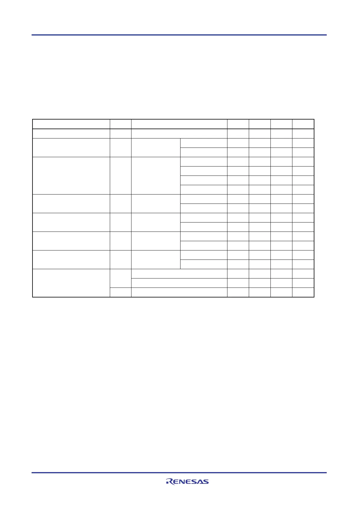
(3) When AV
REF (+) = VDD (ADREFP1 = 0, ADREFP0 = 0), AVREF (−) = VSS (ADREFM = 0), target ANI pin : ANI0 to
ANI14, ANI16 to ANI26
(T
A = −40 to +85°C, 1.6 V ≤ EVDD0 = EVDD1 ≤ VDD ≤ 5.5 V, VSS = EVSS0 = EVSS1 = 0 V, Reference voltage (+) = VDD,
Reference voltage (−) = VSS)
Parameter Symbol Conditions MIN. TYP. MAX. Unit
Resolution RES 8 10 bit
1.8 V ≤ VDD ≤ 5.5 V 1.2 ±7.0 LSB Overall error
Notes 1, 2
AINL 10-bit resolution
1.6 V ≤ V
DD ≤ 5.5 V 1.2 ±10.5 LSB
3.6 V ≤ VDD ≤ 5.5 V 2.125 39
μ
s
2.7 V ≤ VDD ≤ 5.5 V 3.1875 39
μ
s
1.8 V ≤ VDD ≤ 5.5 V 17 39
μ
s
Conversion time tCONV 10-bit resolution
1.6 V ≤ V
DD ≤ 5.5 V 57 95
μ
s
1.8 V ≤ VDD ≤ 5.5 V ±0.60 %FSRZero-scale error
Notes 1, 2
EZS
10-bit resolution
1.6 V ≤ V
DD ≤ 5.5 V ±0.85 %FSR
1.8 V ≤ VDD ≤ 5.5 V ±0.60 %FSRFull-scale error
Notes 1, 2
EFS
10-bit resolution
1.6 V ≤ V
DD ≤ 5.5 V ±0.85 %FSR
1.8 V ≤ VDD ≤ 5.5 V ±4.0 LSB Integral linearity error
Note 1
ILE 10-bit resolution
1.6 V ≤ V
DD ≤ 5.5 V ±6.5 LSB
1.8 V ≤ VDD ≤ 5.5 V ±2.0 LSB Differential linearity error
Note 1
DLE 10-bit resolution
1.6 V ≤ V
DD ≤ 5.5 V ±2.5 LSB
ANI0 to ANI14 0 VDD V VAIN
ANI16 to ANI26 0 EV
DD0 V
Analog input voltage
V
BGR 2.4 V ≤ VDD ≤ 5.5 V 1.38 1.45 1.5 V
Notes 1. Excludes quantization error (±1/2 LSB).
2. This value is indicated as a ratio (%FSR) to the full-scale value.

 Loading...


