7.2
SEL-387-0, -5, -6 Relay Instruction Manual Date Code 20170601
Serial Port Communications and Commands
Establish Communication
Port Identification
If there is ever uncertainty about the number of the port to which you are
connected (1–4), use the command SHO P <Enter>. The relay will respond
with a message identifying the port number, and will list the settings for that
port. The SHO P command is discussed later in more detail.
Cables
Connect the SEL-387 to another device, using the appropriate cable. The pin
definitions for Ports 1, 2, 3, and 4 are given on the relay rear panel and
detailed in Table 7.1.
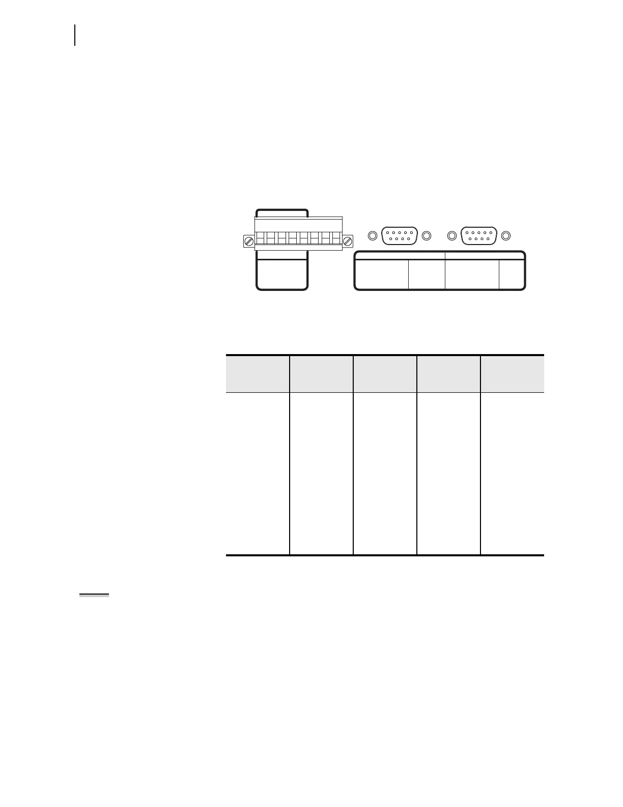
A 9-pin port connector drawing and pin definitions appear in Figure 7.1.
Figure 7.1 SEL-387 Serial Port Connectors
Pinouts for EIA-232 and EIA-485 ports follow:
Port 1 is an EIA-485 protocol connection on the rear of the relay. It accepts a
pluggable terminal block that supports wire sizes from 24 AWG up to
12 AWG. The connector is supplied with the relay. Ports 2, 3, and 4 are
EIA-232 protocol connections with Ports 2 and 3 on the rear of the relay and
Port 4 on the front of the relay. These female connectors are 9-pin, D-
subminiature connectors. Any combination of these ports or all of them may
be used for relay communication. Table 7.2 lists cables that can be purchased
from SEL for various communication applications.
Ta b l e 7.1 S e r i a l P o r t P in D e f i n it i o n s
Pin Number
Port 1 Rear
EIA-485
Port 2 Rear
EIA-232 with
IRIG-B
Port 3 Rear
EIA-232
Port 4 Front
EIA-232
1 +TX (Out) N/C or +5 Vdc* N/C or +5 Vdc* N/C
2 –TX (Out) RXD (In) RXD (In) RXD (In)
3 +RX (In) TXD (Out) TXD (Out) TXD (Out)
4 –RX (In) N/C or
+IRIG-B
a
a
Install a jumper to use the 5 V connection, and remove a solder jumper to disable the IRIG-B
input. See Section 2: Installation for more information.
N/C N/C
5 Shield GND GND GND
6 N/C N/C or
–IRIG-B
a
N/C N/C
7 +IRIG-B RTS (Out) RTS (Out) RTS (Out)
8 –IRIG-B CTS (In) CTS (In) CTS (In)
9 NA GND GND GND
4
5
2
3
1
-RX
SHIELD
+RX
-TX
+TX
PIN EIA-485
SERIAL
1
PORT
2345N/C
1
-IRIG-B
N/C OR +5Vdc
3
4
1
2
PIN
7TXD
+IRIG-B 8
RXD
5,9
6
PIN
RXD
N/C
TXD
N/C OR +5Vdc
RTS 3
CTS 4
PIN
GND 1
2
RTS7
8 CTS
GND5,9
N/C6
PIN
PORT 2 EIA-232
9
1
+
78
-
SERIAL
PORT 2
PORT 3 and 4 EIA-232
9
1
PORT 3
SERIAL
IRIG-B
89
54
67
321
89
54
67
321
NOTE: Listing of devices not
manufactured by SEL is for the
convenience of our customers. SEL
does not specifically endorse or
recommend such products nor does
SEL guarantee proper operation of
those products, or the correctness of
connections, over which SEL has no
control.