UG-570 AD9361 Reference Manual
| Page 122 of 128
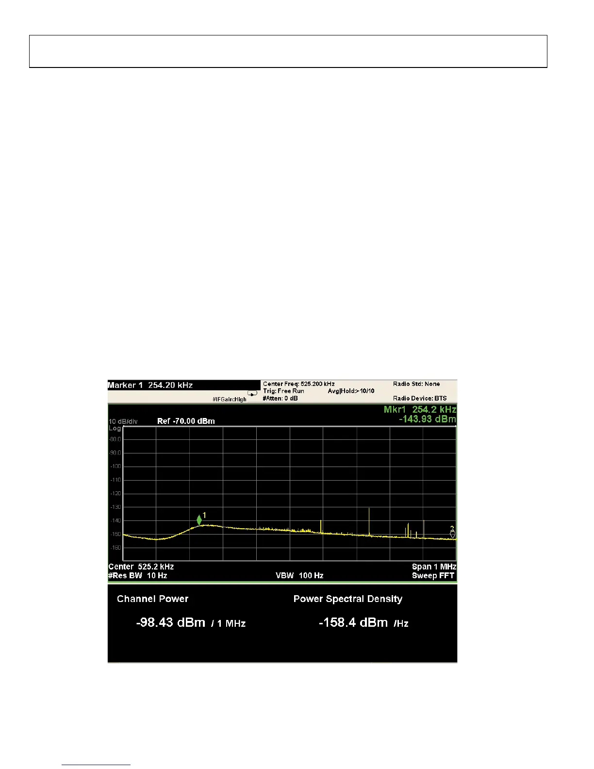
Output Noise Spectrum
Figure 89 shows the output spectrum of the ADP5040 switching
regulator up to 1 MHz. This span is important, as the AD9361
is more sensitive to low frequency noise than it is to high
frequency noise. Switcher noise greater than 1 MHz is also
important. Some switching regulators can have large multiples
of the switching frequency with many sidebands. These spurs
generated by the switcher can couple into other power supplies
or RF balls.
Switching Frequency
The switching frequency of the switching regulator is also an
important characteristic to consider. Figure 90 shows that the
frequency of the power supply noise less than the synthesizer
loop filter bandwidth is the most important. Therefore, choose
a regulator with a switching frequency greater than 1 MHz.
Since the switching frequency of ADP5040 is 3 MHz, it is
relatively quiet ranging from 100 Hz to 500 kHz.
Slew Rate
The slew rate of the regulator is important to control the rise
time and fall times of the switching edges. A switcher regulator
with a high slew rate is preferred as this reduces low frequency
sidebands that can fall below 1 MHz.
Maximum Output Capacitance
In switching regulators with limitation for the maximum
allowable output capacitance, it is important to consider the
effects over the lowest frequency that can be decoupled from
the power supply noise. Two main factors affect the transient
response of a switching regulator: the output capacitor ESR and
the regulator loop bandwidth. To improve the transient
response, it is preferable to add capacitors in parallel instead of
using one larger output capacitor. This is to reduce the total
ESR. Increasing the output capacitance value also changes the
regulator loop characteristics and the phase margin, small phase
margin yields to an under-damped system where oscillation
occurs after a transient. If the phase margin is too large then the
system becomes over-damped where the response to transients
is slow. Transient performance considerations are in the Rx LO
Frequency Deviations Due to Power Supply Transients section.
Figure 89 shows the 1 MHz noise spectrum of the ADP5040. In
this screenshot, the ADP5040 is powering up the 1.3 V analog
power plane with the AD9361 in FDD mode.
Fig
ure 89. Noise Floor at the Buck Output of ADP5040 Powering the1.3 V Analog Plane (The AD9361 in FDD State)

 Loading...


