Functional Description
2-8 Copyright © 2008 ARM Limited. All rights reserved. ARM DDI 0414C
Non-Confidential
Restricted Access
Table 2-5 shows the MBISTBE bits used to control the tag RAMs.
Outer RAM
Outer RAM consists of one array per CPU. It is a bit-writable RAM. Bit-write enables
must be controllable separately.
MBISTARRAY[17] selects the Outer RAM array.
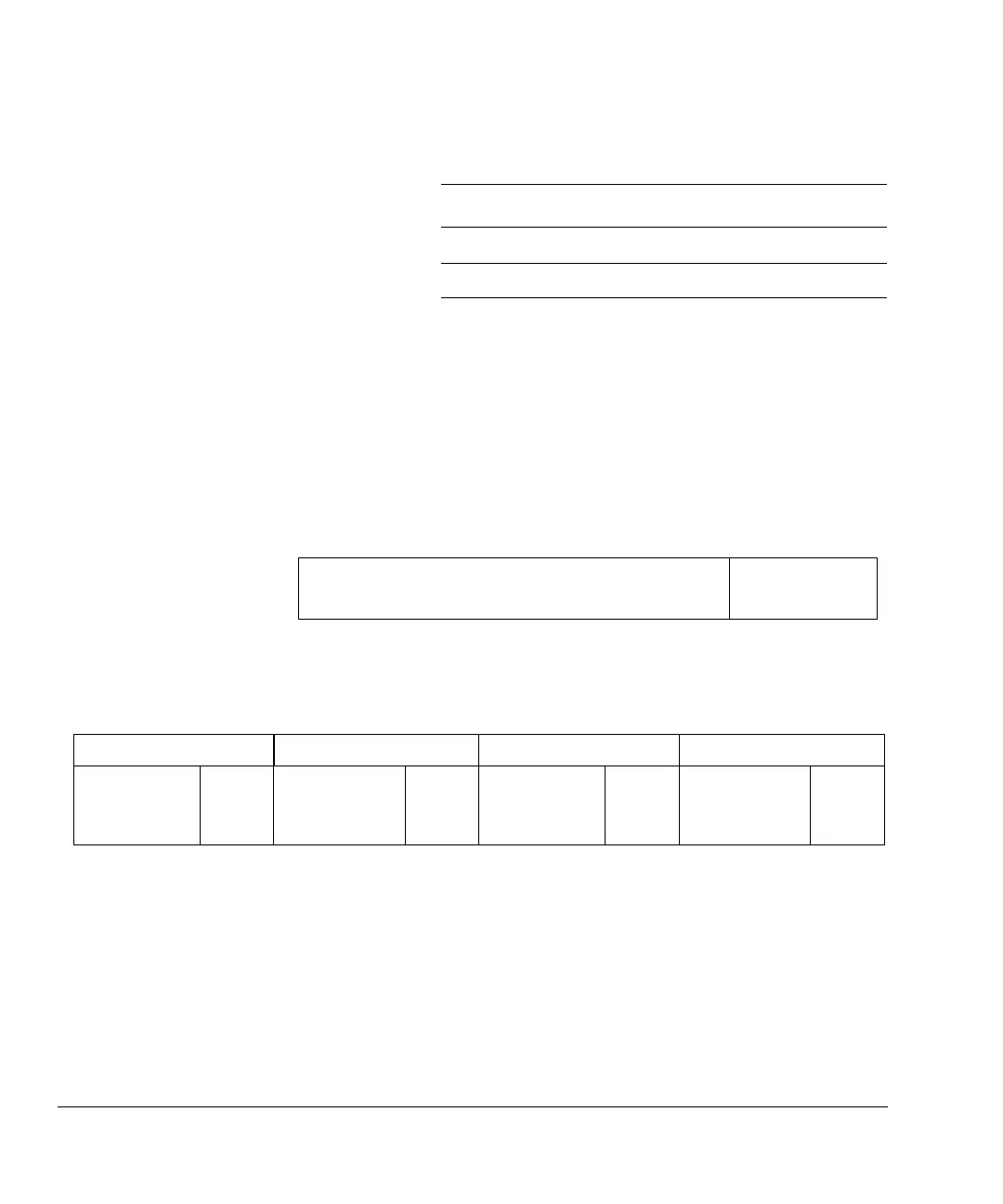
Figure 2-7 and Figure 2-8 show the data mapping on MBISTINDATA and
MBISTOUTDATA buses for Outer RAM.
Figure 2-7 Data in for Outer RAM
Figure 2-8 Data out for Outer RAM
Branch Target Address Cache RAM
Branch Target Address Cache (BTAC) RAMs consist of two arrays, one for control and
one for target. The target array is always 32 bits wide.
MBISTARRAY[1:0] selects the BTAC array. They are word-writable, controlled by
MBISTWRITEEN when in BIST mode.
Table 2-5 Tag RAM control
RAM type Write enable MBISTBE bits
SCU tag RAM Bit-write enable [22:0]
Data tag RAM Bit-write enable [25:0]
MBISTINDATA[63:0]
Outer Data in [11:0]
Unused
3132 063 2728
MBISTOUTDATA[255:0]
63 0127128191192255 64
Unused
Data out
[11:0]
Data out [63:0] for CPU3 Data out [63:0] for CPU2 Data out [63:0] for CPU1 Data out [63:0] for CPU0
Unused
Data out
[11:0]
Unused
Data out
[11:0]
Unused
Data out
[11:0]