Functional Description
ARM DDI 0414C Copyright © 2008 ARM Limited. All rights reserved. 2-5
Restricted Access Non-Confidential
Instruction data and Data data RAMs
The Instruction data cache is selected using bits MBISTARRAY[7:4]. The Data data
cache is selected using bits MBISTARRAY[16:13]. This cache is byte-writable. All
write enable bits must be controllable separately.
Both data caches consist of eight RAM arrays. See RAM arrays and MBIST controller
interfaces on page 2-2 for more information. For both data caches two arrays are tested
in parallel and the same data is sent to each CPU.
For
n=0
to
n=3
Data in and Data out buses are mapped as shown in Figure 2-1 and
Figure 2-2.
Figure 2-1 Data In for Instruction data RAM and Data data RAM
Figure 2-2 Data Out for Instruction data RAM and Data data RAM
Instruction data RAMs have a word write enable, controlled by MBISTWRITEEN
when in BIST mode.
Data data RAMs have a byte write enable, controlled by MBISTBE[3:0] as shown in
Table 2-3.
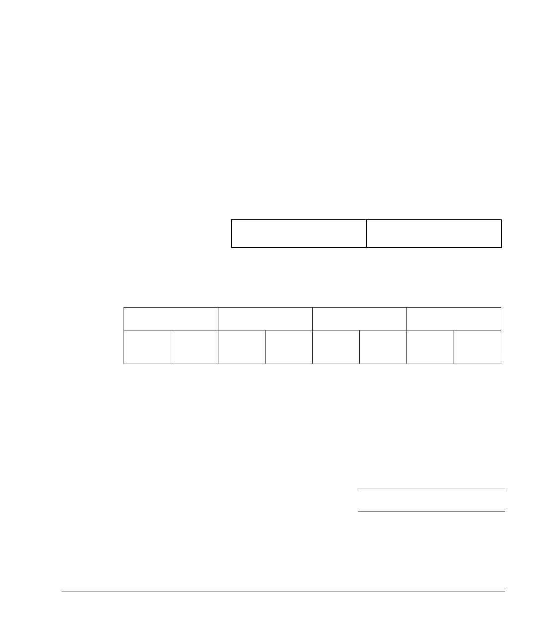
MBISTINDATA[63:0]
Data in [31:0] for array n+1 Data in [31:0] for array n
0
313263
Data out
[31:0] for
array n+1
Data out
[31:0] for
array n
Data out
[31:0] for
array n+1
Data out
[31:0] for
array n
Data out
[31:0] for
array n+1
Data out
[31:0] for
array n
Data out
[31:0] for
array n+1
Data out
[31:0] for
array n
Data out [63:0] for
CPU3
Data out [63:0] for
CPU2
Data out [63:0] for
CPU1
Data out [63:0] for
CPU0
MBISTOUTDATA[255:0]
255 192 191 128 127 64 63 0
Table 2-3 Data data RAM byte write enable control
MBISTBE bit Description
0 Byte 0, bits [7:0]