Functional Description
ARM DDI 0414C Copyright © 2008 ARM Limited. All rights reserved. 2-9
Restricted Access Non-Confidential
Figure 2-9 and Figure 2-10 show the data mapping on MBISTINDATA and
MBISTOUTDATA buses for BTAC RAM.
Figure 2-9 Data in for BTAC RAM
Figure 2-10 Data out for BTAC RAM
TLB RAM
TLB RAM consists of two arrays. MBISTARRAY[10:9] selects these arrays. The TLB
arrays are word-writable, controlled by MBISTWRITEEN when in BIST mode.
Figure 2-11 and Figure 2-12 on page 2-10 show the data mapping on MBISTINDATA
and MBISTOUTDATA buses for TLB RAM.
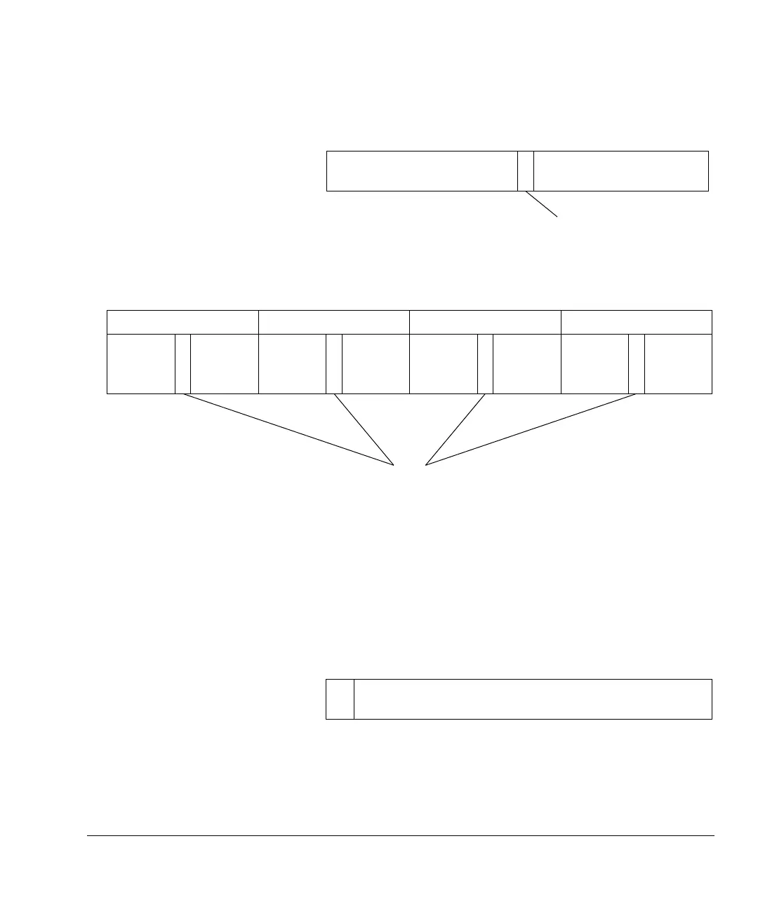
Figure 2-11 Data in for TLB RAM
Data in [27:0] control array
MBISTINDATA[63:0]
Data in [31:0] target array
0
63
30
62
27
Unused
31
MBISTOUTDATA[255:0]
63 0127128191192255 64
Data out
[27:0] for
control array
Data out [63:0] for CPU3 Data out [63:0] for CPU2 Data out [63:0] for CPU1 Data out [63:0] for CPU0
Data out
[31:0] for
target array
Data out
[27:0] for
control array
Data out
[31:0] for
target array
Data out
[27:0] for
control array
Data out
[31:0] for
target array
Data out
[27:0] for
control array
Data out
[31:0] for
target array
Unused
Data in [60:0] for array 0
MBISTINDATA[63:0]
0
63 62
Un-
used
61