Functional Description
2-10 Copyright © 2008 ARM Limited. All rights reserved. ARM DDI 0414C
Non-Confidential
Restricted Access
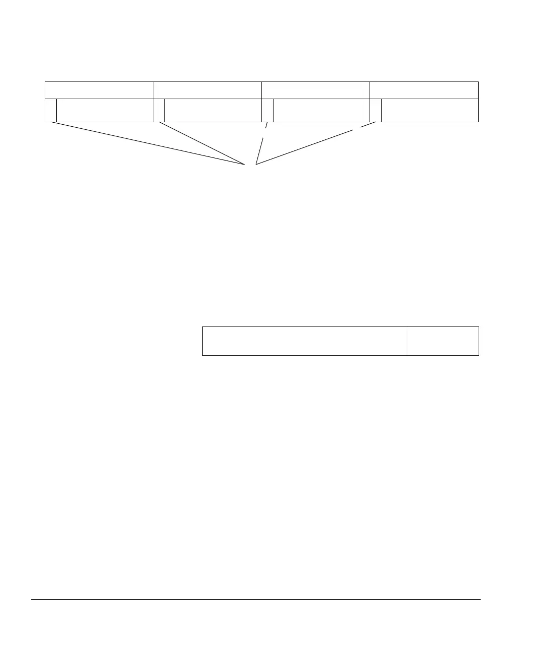
Figure 2-12 Data out for TLB RAM
Global History Buffer RAMs
Global History Buffer (GHB) RAM consists of four arrays which are four bits wide.
Address space is 512 words. MBISTARRAY[8] selects the GHB arrays.
The GHB arrays are bit-writable, controlled by MBISTBE[11:0] when in BIST mode.
Figure 2-13 shows the data mapping on the MBISTINDATA bus for GHB RAM.
Figure 2-13 Data in for GHB RAM
2.1.3 MBIST controller implementation
The MBIST controller block shown in Figure 2-14 on page 2-11 contains two major
blocks:
• MBIST controller
• dispatch unit.
MBISTOUTDATA[255:0]
0128191192255
Data out [60:0]
Data out [63:0] for CPU3 Data out [63:0] for CPU2 Data out [63:0] for CPU1 Data out [63:0] for CPU0
Unused
Data out [60:0] Data out [60:0] Data out [60:0]
127
64 63
GHB Data in [11:0]
MBISTINDATA[63:0]
0
63 32
Unused
31
15