253
2467S–AVR–07/09
ATmega128
Bypass Register The Bypass Register consists of a single Shift Register stage. When the Bypass Register is
selected as path between TDI and TDO, the register is reset to 0 when leaving the Capture-DR
controller state. The Bypass Register can be used to shorten the scan chain on a system when
the other devices are to be tested.
Device Identification
Register
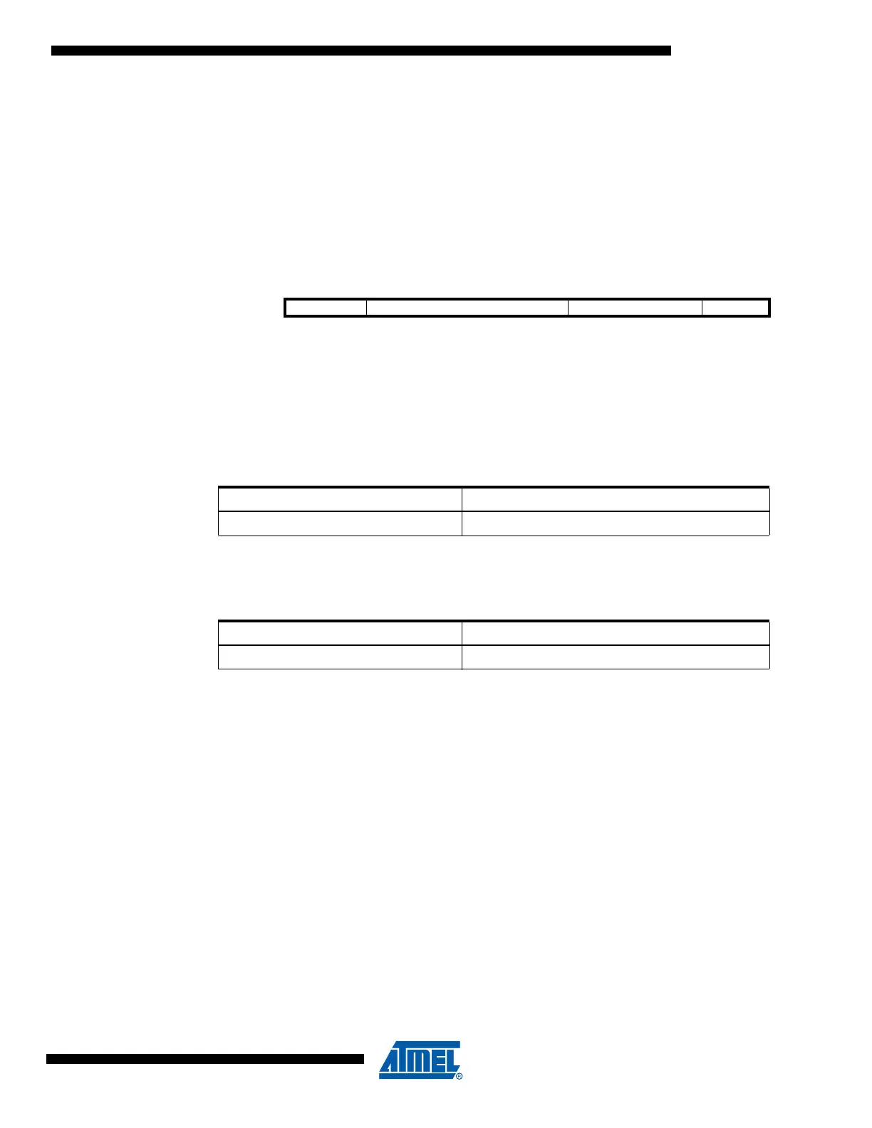
Figure 122 shows the structure of the Device Identification Register.
Figure 122. The Format of the Device Identification Register
Version Version is a 4-bit number identifying the revision of the component. The JTAG version number
follows the revision of the device, and wraps around at revision P (0xF). Revision A and Q is
0x0, revision B and R is 0x1 and so on.
Part Number The part number is a 16-bit code identifying the component. The JTAG Part Number for
ATmega128 is listed in Table 100.
Manufacturer ID The Manufacturer ID is a 11-bit code identifying the manufacturer. The JTAG manufacturer ID
for ATMEL is listed in Table 101.
Reset Register The Reset Register is a Test Data Register used to reset the part. Since the AVR tri-states Port
Pins when reset, the Reset Register can also replace the function of the unimplemented optional
JTAG instruction HIGHZ.
A high value in the Reset Register corresponds to pulling the External Reset low. The part is
reset as long as there is a high value present in the Reset Register. Depending on the Fuse set-
tings for the clock options, the part will remain reset for a Reset Time-Out Period (refer to “Clock
Sources” on page 37) after releasing the Reset Register. The output from this Data Register is
not latched, so the Reset will take place immediately, as shown in Figure 123.
MSB
LSB
Bit
31 28 27 12 11 1 0
Device ID Version Part Number Manufacturer ID 1
4 bits 16 bits 11 bits 1-bit
Table 100. AVR JTAG Part Number
Part Number JTAG Part Number (Hex)
ATmega128 0x9702
Table 101. Manufacturer ID
Manufacturer JTAG Manufacturer ID (Hex)
ATME L 0x0 1 F