261
2467S–AVR–07/09
ATmega128
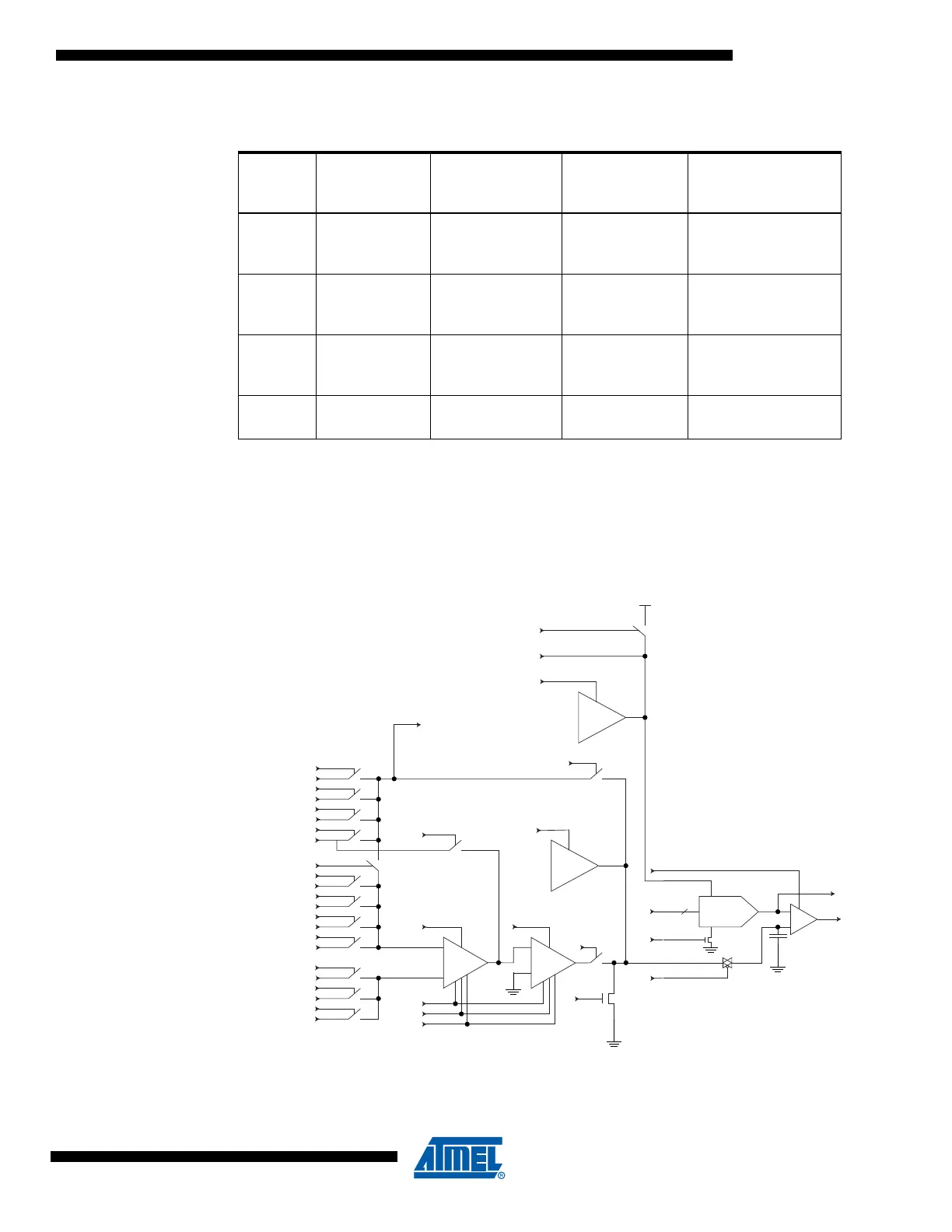
Scanning the ADC Figure 131 shows a block diagram of the ADC with all relevant control and observe signals. The
Boundary-scan cell from Figure 127 is attached to each of these signals. The ADC need not be
used for pure connectivity testing, since all analog inputs are shared with a digital port pin as
well.
Figure 131. Analog to Digital Converter
The signals are described briefly in Table 104.
Table 103. Boundary-scan Signals for the Analog Comparator
Signal
Name
Direction as
Seen from the
Comparator Description
Recommended
Input when not
in Use
Output values when
Recommended
Inputs are Used
AC_IDLE Input Turns off Analog
comparator when
true
1 Depends upon µC
code being executed
ACO Output Analog
Comparator
Output
Will become
input to µC code
being executed
0
ACME Input Uses output
signal from ADC
mux when true
0 Depends upon µC
code being executed
ACBG Input Bandgap
Reference enable
0 Depends upon µC
code being executed
10-bit DAC +
-
AREF
PRECH
DACOUT
COMP
MUXEN_7
ADC_7
MUXEN_6
ADC_6
MUXEN_5
ADC_5
MUXEN_4
ADC_4
MUXEN_3
ADC_3
MUXEN_2
ADC_2
MUXEN_1
ADC_1
MUXEN_0
ADC_0
NEGSEL_2
ADC_2
NEGSEL_1
ADC_1
NEGSEL_0
ADC_0
EXTCH
+
-
+
-
10x 20x
G10
G20
ST
ACLK
AMPEN
2.56V
ref
IREFEN
AREF
VCCREN
DAC_9..0
ADCEN
HOLD
PRECH
GNDEN
PASSEN
ACTEN
COMP
SCTEST
ADCBGEN
To Comparator
1.22V
ref
AREF