300
2467S–AVR–07/09
ATmega128
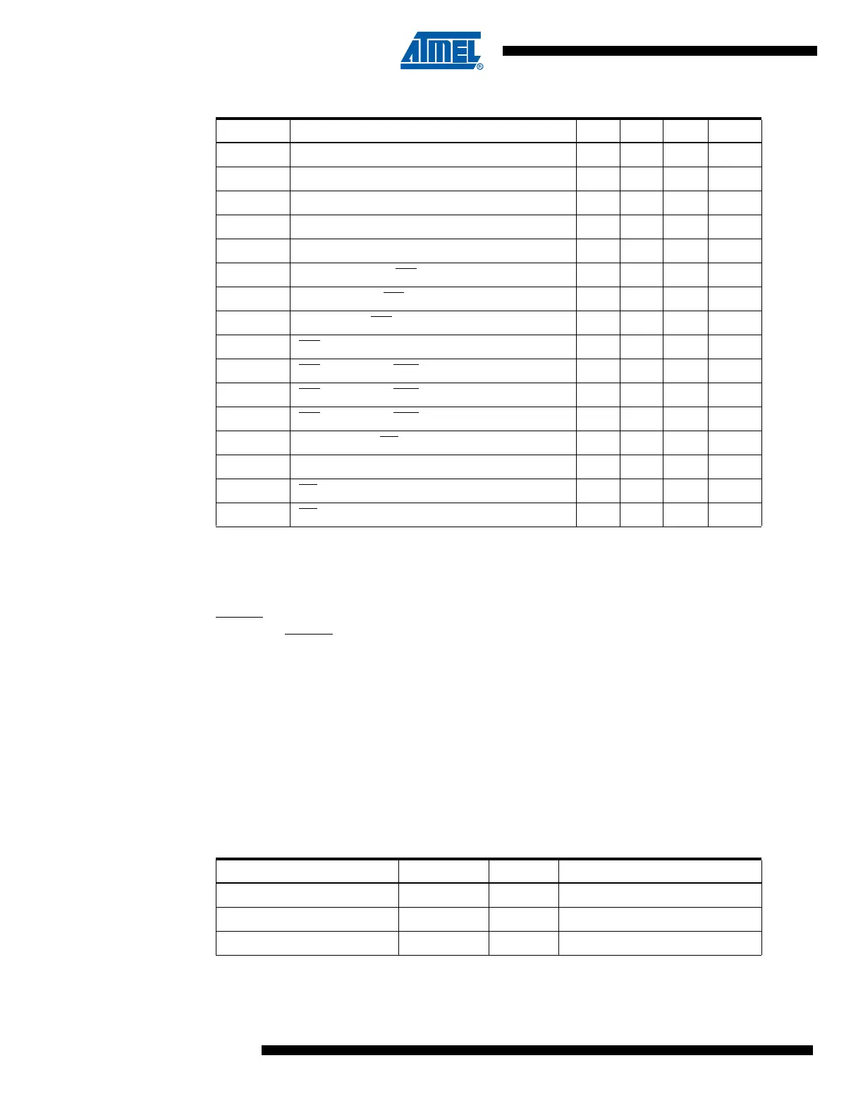
Notes: 1. t
WLRH
is valid for the Write Flash, Write EEPROM, Write Fuse bits and Write Lock bits
commands.
2. t
WLRH_CE
is valid for the Chip Erase command.
Serial
Downloading
Both the Flash and EEPROM memory arrays can be programmed using the serial SPI bus while
RESET
is pulled to GND. The serial interface consists of pins SCK, MOSI (input) and MISO (out-
put). After RESET
is set low, the Programming Enable instruction needs to be executed first
before program/erase operations can be executed. NOTE, in Table 127 on page 300, the pin
mapping for SPI programming is listed. Not all parts use the SPI pins dedicated for the internal
SPI interface. Note that throughout the description about Serial downloading, MOSI and MISO
are used to describe the serial data in and serial data out respectively. For ATmega128 these
pins are mapped to PDI and PDO.
SPI Serial
Programming Pin
Mapping
Even though the SPI Programming interface re-uses the SPI I/O module, there is one important
difference: The MOSI/MISO pins that are mapped to PB2 and PB3 in the SPI I/O module are not
used in the Programming interface. Instead, PE0 and PE1 are used for data in SPI Program-
ming mode as shown in Table 127.
t
XLPH
XTAL1 Low to PAGEL high 0 ns
t
PLXH
PAGEL low to XTAL1 high 150 ns
t
BVPH
BS1 Valid before PAGEL High 67 ns
t
PHPL
PAGEL Pulse Width High 150 ns
t
PLBX
BS1 Hold after PAGEL Low 67 ns
t
WLBX
BS2/1 Hold after WR Low 67 ns
t
PLWL
PAGEL Low to WR Low 67 ns
t
BVWL
BS1 Valid to WR Low 67 ns
t
WLWH
WR Pulse Width Low 150 ns
t
WLRL
WR Low to RDY/BSY Low 0 1 μs
t
WLRH
WR Low to RDY/BSY High
(1)
3.7 5 ms
t
WLRH_CE
WR Low to RDY/BSY High for Chip Erase
(2)
7.5 10 ms
t
XLOL
XTAL1 Low to OE Low 0 ns
t
BVDV
BS1 Valid to DATA valid 0 250 ns
t
OLDV
OE Low to DATA Valid 250 ns
t
OHDZ
OE High to DATA Tri-stated 250 ns
Table 126. Parallel Programming Characteristics, V
CC
= 5 V ± 10% (Continued)
Symbol Parameter Min Typ Max Units
Table 127. Pin Mapping SPI Serial Programming
Symbol Pins I/O Description
MOSI (PDI) PE0 I Serial data in
MISO (PDO) PE1 O Serial data out
SCK PB1 I Serial clock