31
2467S–AVR–07/09
ATmega128
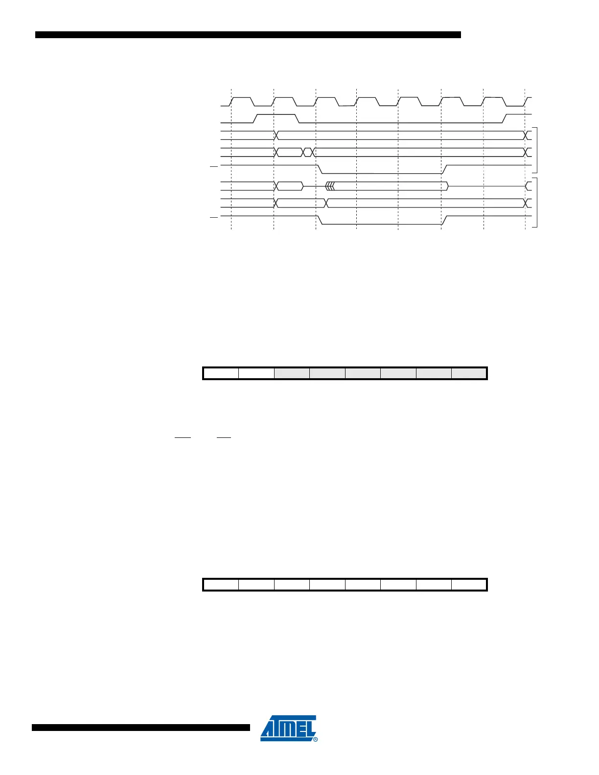
Figure 16. External Data Memory Cycles with SRWn1 = 1 and SRWn0 = 1
(1)
Note: 1. SRWn1 = SRW11 (upper sector) or SRW01 (lower sector), SRWn0 = SRW10 (upper sector) or
SRW00 (lower sector).
The ALE pulse in period T7 is only present if the next instruction accesses the RAM (internal
or external).
XMEM Register
Description
MCU Control Register
– MCUCR
• Bit 7 – SRE: External SRAM/XMEM Enable
Writing SRE to one enables the External Memory Interface.The pin functions AD7:0, A15:8,
ALE, WR
, and RD are activated as the alternate pin functions. The SRE bit overrides any pin
direction settings in the respective data direction registers. Writing SRE to zero, disables the
External Memory Interface and the normal pin and data direction settings are used.
• Bit 6 – SRW10: Wait-state Select Bit
For a detailed description in non-ATmega103 compatibility mode, see common description for
the SRWn bits below (XMCRA description). In ATmega103 compatibility mode, writing SRW10
to one enables the wait-state and one extra cycle is added during read/write strobe as shown in
Figure 14.
External Memory
Control Register A –
XMCRA
• Bit 7 – Res: Reserved Bit
This is a reserved bit and will always read as zero. When writing to this address location, write
this bit to zero for compatibility with future devices.
ALE
T1 T2 T3
Write
Read
WR
T7
A15:8
AddressPrev. addr.
DA7:0
Address DataPrev. data XX
RD
DA7:0 (XMBK = 0)
DataPrev. data Address
DataPrev. data Address
DA7:0 (XMBK = 1)
System Clock (CLK
CPU
)
T4 T5 T6
Bit 76543210
SRE SRW10
SE SM1 SM0 SM2 IVSEL IVCE MCUCR
Read/Write R/W R/W R/W R/W R/W R/W R/W R/W
Initial Value00000000
Bit 76543210
– SRL2 SRL1 SRL0 SRW01 SRW00 SRW11 – XMCRA
Read/Write R R/W R/W R/W R/W R/W R/W R
Initial Value00000000