2
2467S–AVR–07/09
ATmega128
Pin
Configurations
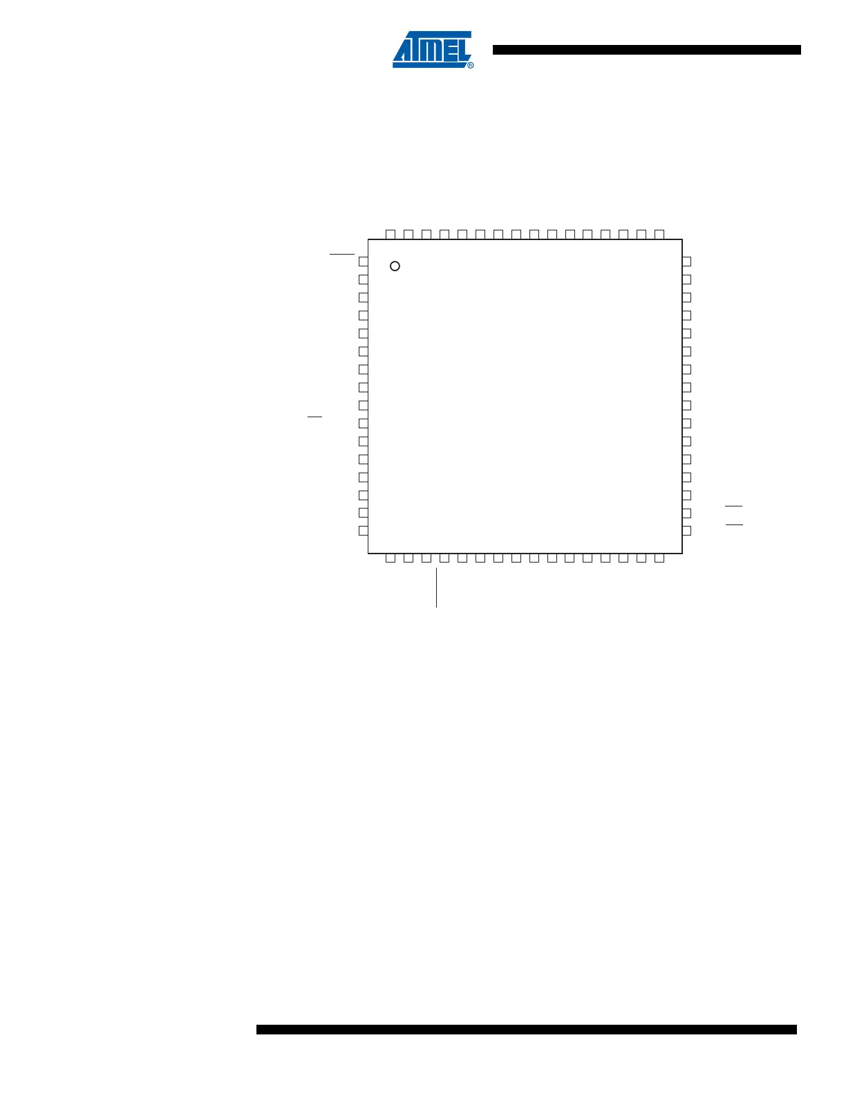
Figure 1. Pinout ATmega128
Note: The Pinout figure applies to both TQFP and MLF packages. The bottom pad under the QFN/MLF
package should be soldered to ground.
Overview The ATmega128 is a low-power CMOS 8-bit microcontroller based on the AVR enhanced RISC
architecture. By executing powerful instructions in a single clock cycle, the ATmega128
achieves throughputs approaching 1 MIPS per MHz allowing the system designer to optimize
power consumption versus processing speed.
1
2
3
4
5
6
7
8
9
10
11
12
13
14
15
16
48
47
46
45
44
43
42
41
40
39
38
37
36
35
34
33
PEN
RXD0/(PDI) PE0
(TXD0/PDO) PE1
(XCK0/AIN0) PE2
(OC3A/AIN1) PE3
(OC3B/INT4) PE4
(OC3C/INT5) PE5
(T3/INT6) PE6
(ICP3/INT7) PE7
(SS) PB0
(SCK) PB1
(MOSI) PB2
(MISO) PB3
(OC0) PB4
(OC1A) PB5
(OC1B) PB6
PA3 (AD3)
PA4 (AD4)
PA5 (AD5)
PA6 (AD6)
PA7 (AD7)
PG2(ALE)
PC7 (A15)
PC6 (A14)
PC5 (A13)
PC4 (A12)
PC3 (A11)
PC2 (A10)
PC1 (A9)
PC0 (A8)
PG1(RD)
PG0(WR)
64
63
62
61
60
59
58
57
56
55
54
53
52
51
50
49
17
18
19
20
21
22
23
24
25
26
27
28
29
30
31
32
(OC2/OC1C) PB7
TOSC2/PG3
TOSC1/PG4
RESET
VCC
GND
XTAL2
XTAL1
(SCL/INT0) PD0
(SDA/INT1) PD1
(RXD1/INT2) PD2
(TXD1/INT3) PD3
(ICP1) PD4
(XCK1) PD5
(T1) PD6
(T2) PD7
AVCC
GND
AREF
PF0 (ADC0)
PF1 (ADC1)
PF2 (ADC2)
PF3 (ADC3)
PF4 (ADC4/TCK)
PF5 (ADC5/TMS)
PF6 (ADC6/TDO)
PF7 (ADC7/TDI)
GND
VCC
PA0 (AD0)
PA1 (AD1)
PA2 (AD2)