69
2467S–AVR–07/09
ATmega128
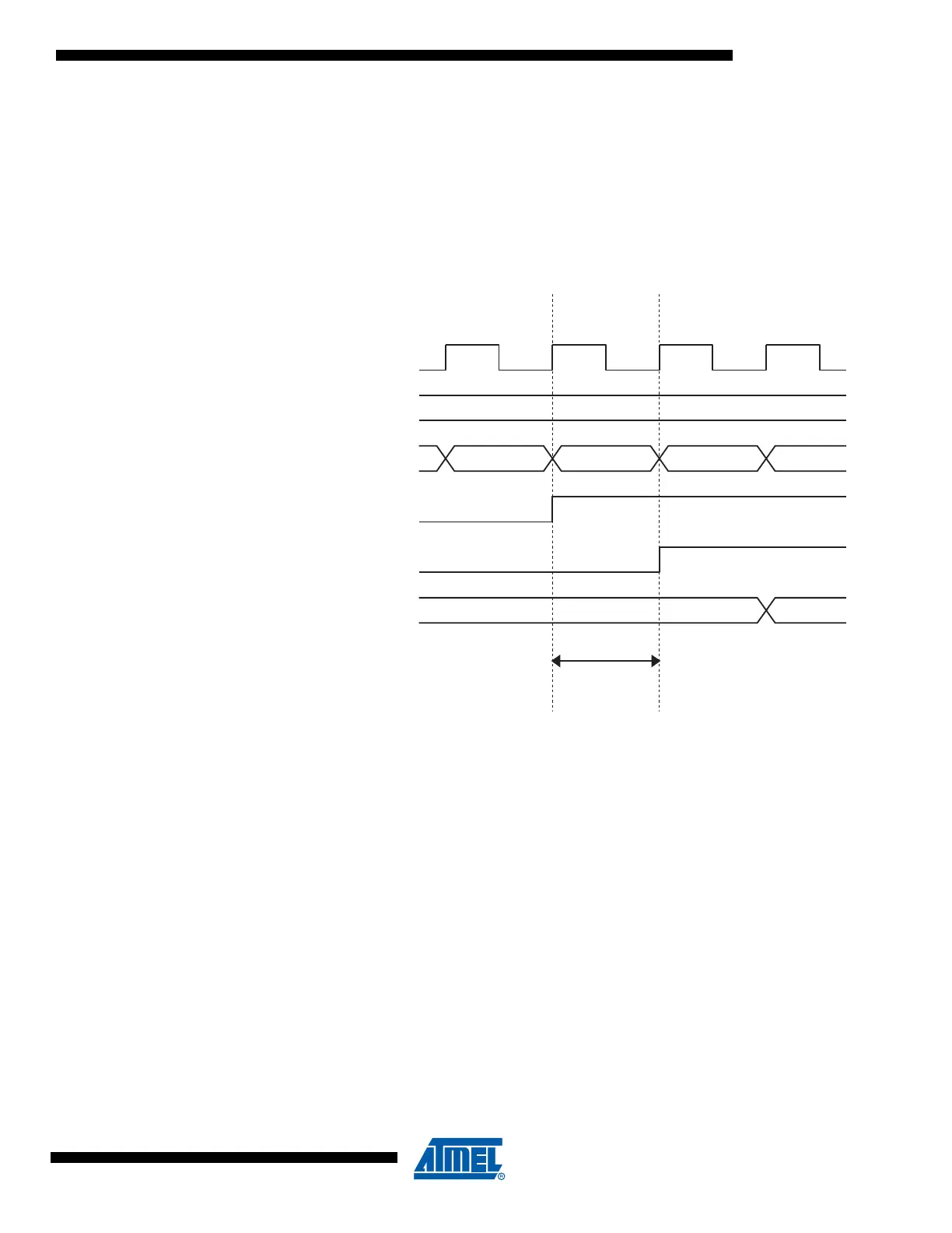
shaded region of the “SYNC LATCH” signal. The signal value is latched when the system clock
goes low. It is clocked into the PINxn Register at the succeeding positive clock edge. As indi-
cated by the two arrows t
pd,max
and t
pd,min
, a single signal transition on the pin will be delayed
between ½ and 1½ system clock period depending upon the time of assertion.
When reading back a software assigned pin value, a nop instruction must be inserted as indi-
cated in Figure 32. The out instruction sets the “SYNC LATCH” signal at the positive edge of the
clock. In this case, the delay t
pd
through the synchronizer is one system clock period.
Figure 32. Synchronization when Reading a Software Assigned Pin Value
nop in r17, PINx
0xFF
0x00
0xFF
t
pd
out PORTx, r16
SYSTEM CLK
r16
INSTRUCTIONS
SYNC LATCH
PINxn
r17