106
2467S–AVR–07/09
ATmega128
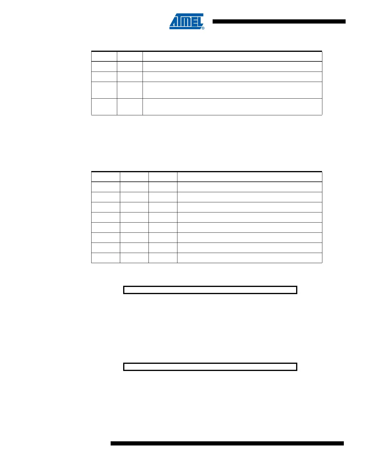
Note: 1. A special case occurs when OCR0 equals TOP and COM01 is set. In this case, the compare
match is ignored, but the set or clear is done at TOP. See “Phase Correct PWM Mode” on page
101 for more details.
• Bit 2:0 – CS02:0: Clock Select
The three clock select bits select the clock source to be used by the Timer/Counter, see Table
56.
Timer/Counter
Register – TCNT0
The Timer/Counter Register gives direct access, both for read and write operations, to the
Timer/Counter unit 8-bit counter. Writing to the TCNT0 Register blocks (removes) the compare
match on the following timer clock. Modifying the counter (TCNT0) while the counter is running,
introduces a risk of missing a compare match between TCNT0 and the OCR0 Register.
Output Compare
Register – OCR0
The Output Compare Register contains an 8-bit value that is continuously compared with the
counter value (TCNT0). A match can be used to generate an output compare interrupt, or to
generate a waveform output on the OC0 pin.
Table 55. Compare Output Mode, Phase Correct PWM Mode
(1)
COM01 COM00 Description
0 0 Normal port operation, OC0 disconnected.
01Reserved
1 0 Clear OC0 on compare match when up-counting. Set OC0 on compare
match when downcounting.
1 1 Set OC0 on compare match when up-counting. Clear OC0 on compare
match when downcounting.
Table 56. Clock Select Bit Description
CS02 CS01 CS00 Description
0 0 0 No clock source (Timer/Counter stopped)
001clk
T0S
/(No prescaling)
010
clk
T0S
/8 (From prescaler)
011
clk
T0S
/32 (From prescaler)
100
clk
T0S
/64 (From prescaler)
101
clk
T0S
/128 (From prescaler)
110clk
T
0
S
/256 (From prescaler)
111clk
T
0
S
/1024 (From prescaler)
Bit 76543210
TCNT0[7:0] TCNT0
Read/Write R/W R/W R/W R/W R/W R/W R/W R/W
Initial Value00000000
Bit 76543210
OCR0[7:0] OCR0
Read/Write R/W R/W R/W R/W R/W R/W R/W R/W
Initial Value00000000