262
2467S–AVR–07/09
ATmega128
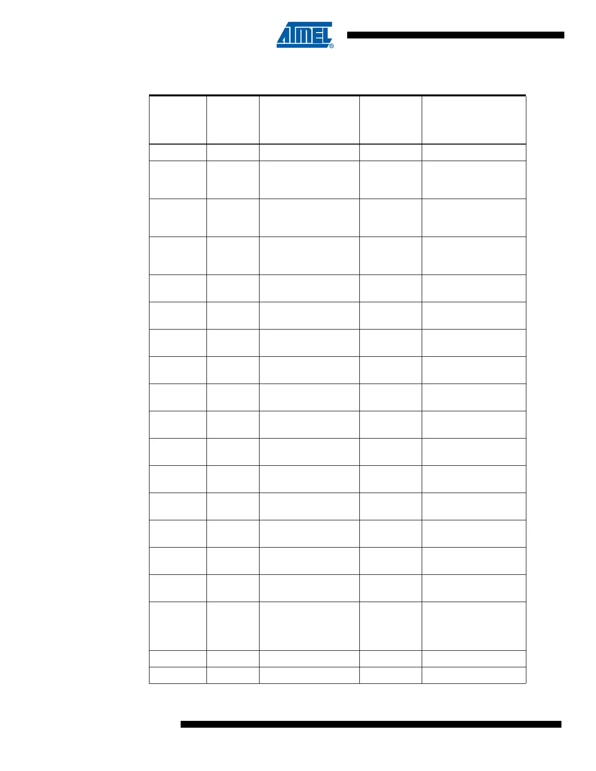
Table 104. Boundary-scan Signals for the ADC
Signal
Name
Direction
as Seen
from the
ADC Description
Recommen-
ded Input
when not
in Use
Output Values when
Recommended Inputs
are Used, and CPU is
not Using the ADC
COMP Output Comparator Output 0 0
ACLK Input Clock signal to gain
stages implemented
as Switch-cap filters
00
ACTEN Input Enable path from gain
stages to the
comparator
00
ADCBGEN Input Enable Band-gap
reference as negative
input to comparator
00
ADCEN Input Power-on signal to the
ADC
00
AMPEN Input Power-on signal to the
gain stages
00
DAC_9 Input Bit 9 of digital value to
DAC
11
DAC_8 Input Bit 8 of digital value to
DAC
00
DAC_7 Input Bit 7 of digital value to
DAC
00
DAC_6 Input Bit 6 of digital value to
DAC
00
DAC_5 Input Bit 5 of digital value to
DAC
00
DAC_4 Input Bit 4 of digital value to
DAC
00
DAC_3 Input Bit 3 of digital value to
DAC
00
DAC_2 Input Bit 2 of digital value to
DAC
00
DAC_1 Input Bit 1 of digital value to
DAC
00
DAC_0 Input Bit 0 of digital value to
DAC
00
EXTCH Input Connect ADC
channels 0 - 3 to by-
pass path around gain
stages
11
G10 Input Enable 10x gain 0 0
G20 Input Enable 20x gain 0 0