82
2467S–AVR–07/09
ATmega128
XCK0, USART0 External clock. The Data Direction Register (DDE2) controls whether the clock
is output (DDE2 set) or input (DDE2 cleared). The XCK0 pin is active only when the USART0
operates in Synchronous mode.
• PDO/TXD0 – Port E, Bit 1
PDO, SPI Serial Programming Data Output. During Serial Program Downloading, this pin is
used as data output line for the ATmega128.
TXD0, UART0 Transmit pin.
• PDI/RXD0 – Port E, Bit 0
PDI, SPI Serial Programming Data Input. During Serial Program Downloading, this pin is used
as data input line for the ATmega128.
RXD0, USART0 Receive Pin. Receive Data (Data input pin for the USART0). When the
USART0 receiver is enabled this pin is configured as an input regardless of the value of DDRE0.
When the USART0 forces this pin to be an input, a logical one in PORTE0 will turn on the inter-
nal pull-up.
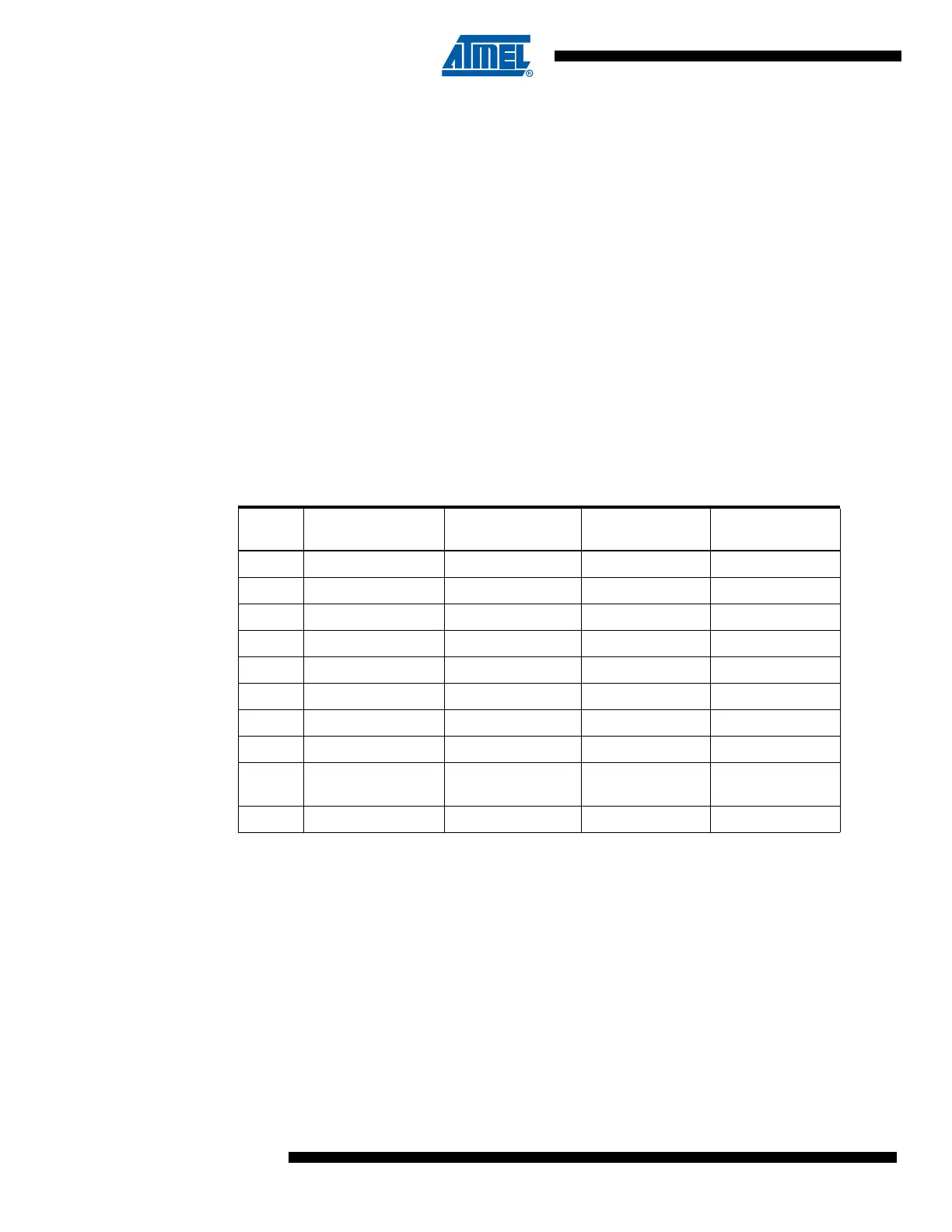
Table 40 and Table 41 relates the alternate functions of Port E to the overriding signals shown in
Figure 33 on page 71.
Table 40. Overriding Signals for Alternate Functions PE7..PE4
Signal
Name PE7/INT7/ICP3 PE6/INT6/T3 PE5/INT5/OC3C PE4/INT4/OC3B
PUOE 0 0 0 0
PUOV 0 0 0 0
DDOE 0 0 0 0
DDOV 0 0 0 0
PVOE 0 0 OC3C ENABLE OC3B ENABLE
PVOV 0 0 OC3C OC3B
DIEOE INT7 ENABLE INT6 ENABLE INT5 ENABLE INT4 ENABLE
DIEOV 1 1 1 1
DI INT7 INPUT/ICP3
INPUT
INT7 INPUT/T3
INPUT
INT5 INPUT INT4 INPUT
AIO – – – –