170
2467S–AVR–07/09
ATmega128
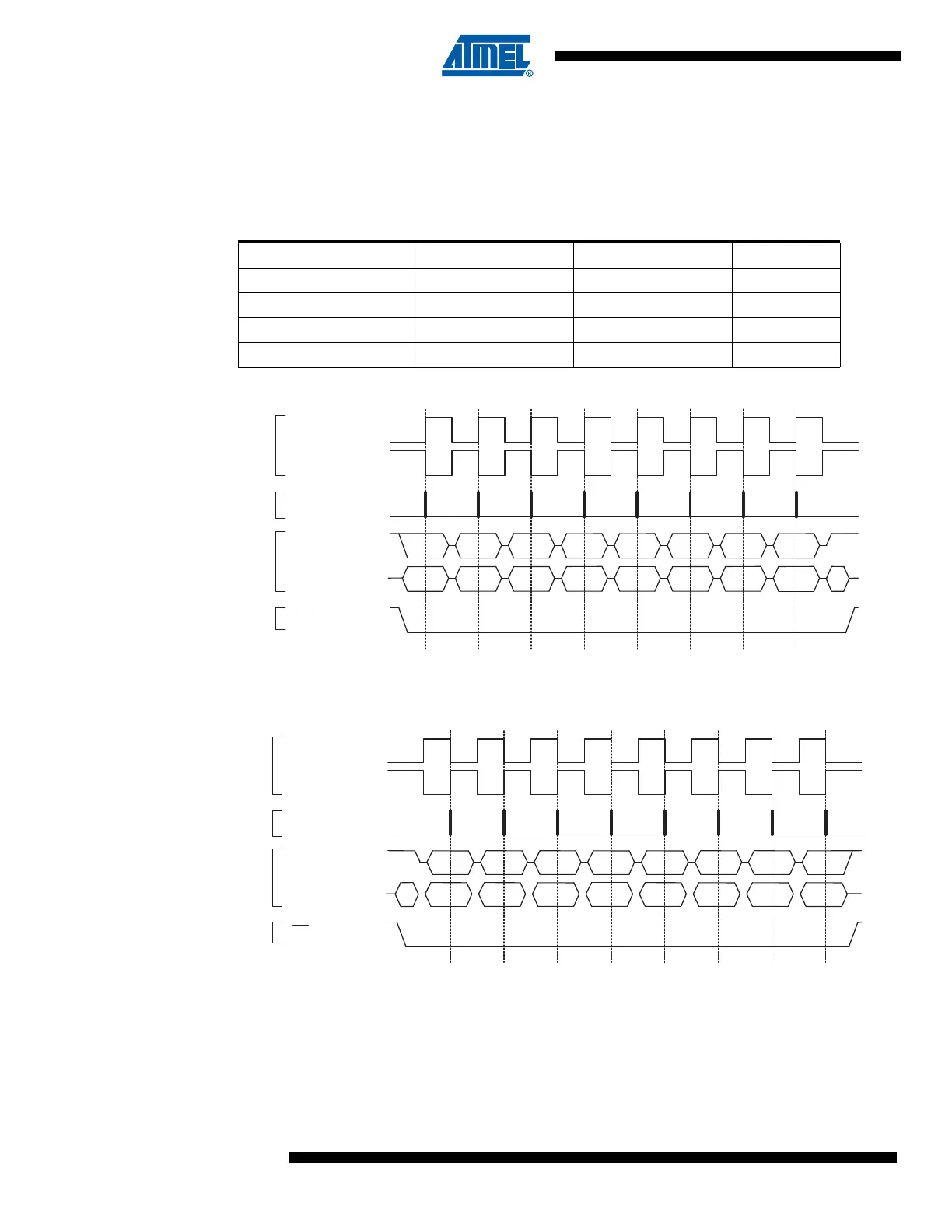
Data Modes There are four combinations of SCK phase and polarity with respect to serial data, which are
determined by control bits CPHA and CPOL. The SPI data transfer formats are shown in Figure
77 and Figure 78. Data bits are shifted out and latched in on opposite edges of the SCK signal,
ensuring sufficient time for data signals to stabilize. This is clearly seen by summarizing Table
70 and Table 71, as done below:
Figure 77. SPI Transfer Format with CPHA = 0
Figure 78. SPI Transfer Format with CPHA = 1
Table 73. CPOL and CPHA Functionality
Leading edge Trailing edge SPI mode
CPOL = 0, CPHA = 0 Sample (Rising) Setup (Falling) 0
CPOL = 0, CPHA = 1 Setup (Rising) Sample (Falling) 1
CPOL = 1, CPHA = 0 Sample (Falling) Setup (Rising) 2
CPOL = 1, CPHA = 1 Setup (Falling) Sample (Rising) 3
Bit 1
Bit 6
LSB
MSB
SCK (CPOL = 0)
mode 0
SAMPLE I
MOSI/MISO
CHANGE 0
MOSI PIN
CHANGE 0
MISO PIN
SCK (CPOL = 1)
mode 2
SS
MSB
LSB
Bit 6
Bit 1
Bit 5
Bit 2
Bit 4
Bit 3
Bit 3
Bit 4
Bit 2
Bit 5
MSB first (DORD = 0)
LSB first (DORD = 1)
SCK (CPOL = 0)
mode 1
SAMPLE I
MOSI/MISO
CHANGE 0
MOSI PIN
CHANGE 0
MISO PIN
SCK (CPOL = 1)
mode 3
SS
MSB
LSB
Bit 6
Bit 1
Bit 5
Bit 2
Bit 4
Bit 3
Bit 3
Bit 4
Bit 2
Bit 5
Bit 1
Bit 6
LSB
MSB
MSB first (DORD = 0)
LSB first (DORD = 1)