238
2467S–AVR–07/09
ATmega128
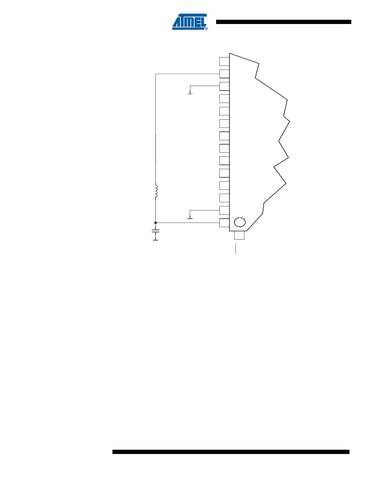
Figure 114. ADC Power Connections
Offset Compensation
Schemes
The gain stage has a built-in offset cancellation circuitry that nulls the offset of differential mea-
surements as much as possible. The remaining offset in the analog path can be measured
directly by selecting the same channel for both differential inputs. This offset residue can be then
subtracted in software from the measurement results. Using this kind of software based offset
correction, offset on any channel can be reduced below one LSB.
VCC
GND
100nF
(ADC0) PF0
(ADC7) PF7
(ADC1) PF1
(ADC2) PF2
(ADC3) PF3
(ADC4) PF4
(ADC5) PF5
(ADC6) PF6
AREF
GND
AVCC
52
53
54
55
56
57
58
59
60
6161
6262
6363
6464
1
51
PEN
(AD0) PA0
10µH