227
2467S–AVR–07/09
ATmega128
Analog
Comparator
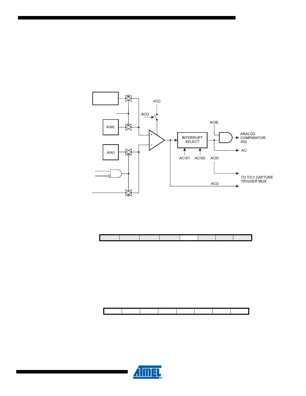
The Analog Comparator compares the input values on the positive pin AIN0 and negative pin
AIN1. When the voltage on the positive pin AIN0 is higher than the voltage on the negative pin
AIN1, the Analog Comparator Output, ACO, is set. The comparator’s output can be set to trigger
the Timer/Counter1 Input Capture function. In addition, the comparator can trigger a separate
interrupt, exclusive to the Analog Comparator. The user can select Interrupt triggering on com-
parator output rise, fall or toggle. A block diagram of the comparator and its surrounding logic is
shown in Figure 107.
Figure 107. Analog Comparator Block Diagram
Notes: 1. See Table 94 on page 229.
2. Refer to Figure 1 on page 2 and Table 39 on page 81 for Analog Comparator pin placement.
Special Function IO
Register – SFIOR
• Bit 3 – ACME: Analog Comparator Multiplexer Enable
When this bit is written logic one and the ADC is switched off (ADEN in ADCSRA is zero), the
ADC multiplexer selects the negative input to the Analog Comparator. When this bit is written
logic zero, AIN1 is applied to the negative input of the Analog Comparator. For a detailed
description of this bit, see “Analog Comparator Multiplexed Input” on page 228.
Analog Comparator
Control and Status
Register – ACSR
• Bit 7 – ACD: Analog Comparator Disable
When this bit is written logic one, the power to the Analog Comparator is switched off. This bit
can be set at any time to turn off the Analog Comparator. This will reduce power consumption in
Active and Idle mode. When changing the ACD bit, the Analog Comparator Interrupt must be
ACBG
BANDGAP
REFERENCE
ADC MULTIPLEXER
OUTPUT
ACME
ADEN
1)
Bit 7 6 5 4 3 2 1 0
TSM – – – ACME PUD PSR0 PSR321 SFIOR
Read/Write R/W R R R R/W R/W R/W R/W
Initial Value 0 0 0 0 0 0 0 0
Bit 76543210
ACD ACBG ACO ACI ACIE ACIC ACIS1 ACIS0 ACSR
Read/Write R/W R/W R R/W R/W R/W R/W R/W
Initial Value00N/A00000