83
2467S–AVR–07/09
ATmega128
Alternate Functions of
Port F
The Port F has an alternate function as analog input for the ADC as shown in Table 42. If some
Port F pins are configured as outputs, it is essential that these do not switch when a conversion
is in progress. This might corrupt the result of the conversion. In ATmega103 compatibility mode
Port F is input only. If the JTAG interface is enabled, the pull-up resistors on pins PF7(TDI),
PF5(TMS), and PF4(TCK) will be activated even if a Reset occurs.
• TDI, ADC7 – Port F, Bit 7
ADC7, Analog to Digital Converter, Channel 7
.
TDI, JTAG Test Data In: Serial input data to be shifted in to the Instruction Register or Data Reg-
ister (scan chains). When the JTAG interface is enabled, this pin can not be used as an I/O pin.
• TDO, ADC6 – Port F, Bit 6
ADC6, Analog to Digital Converter, Channel 6
.
TDO, JTAG Test Data Out: Serial output data from Instruction Register or Data Register. When
the JTAG interface is enabled, this pin can not be used as an I/O pin.
The TDO pin is tri-stated unless TAP states that shift out data are entered.
• TMS, ADC5 – Port F, Bit 5
ADC5, Analog to Digital Converter, Channel 5
.
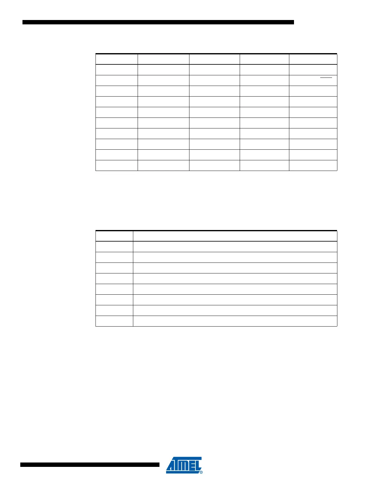
Table 41. Overriding Signals for Alternate Functions in PE3..PE0
Signal Name PE3/AIN1/OC3A PE2/AIN0/XCK0 PE1/PDO/TXD0 PE0/PDI/RXD0
PUOE 0 0 TXEN0 RXEN0
PUOV 0 0 0 PORTE0 • PUD
DDOE 0 0 TXEN0 RXEN0
DDOV 0 0 1 0
PVOE OC3B ENABLE UMSEL0 TXEN0 0
PVOV OC3B XCK0 OUTPUT TXD0 0
DIEOE 0 0 0 0
DIEOV 0 0 0 0
DI 0 XCK0 INPUT – RXD0
AIO AIN1 INPUT AIN0 INPUT – –
Table 42. Port F Pins Alternate Functions
Port Pin Alternate Function
PF7 ADC7/TDI (ADC input channel 7 or JTAG Test Data Input)
PF6 ADC6/TDO (ADC input channel 6 or JTAG Test Data Output)
PF5 ADC5/TMS (ADC input channel 5 or JTAG Test Mode Select)
PF4 ADC4/TCK (ADC input channel 4 or JTAG Test ClocK)
PF3 ADC3 (ADC input channel 3)
PF2 ADC2 (ADC input channel 2)
PF1 ADC1 (ADC input channel 1)
PF0 ADC0 (ADC input channel 0)